SLVSFF0B June   2020  – July 2022 DRV8436E

PRODUCTION DATA  

  1. Features
  2. Applications
  3. Description
  4. Revision History
    1.     Device Options
  5. Pin Configuration and Functions
  6. Specifications
    1. 6.1 Absolute Maximum Ratings
    2. 6.2 ESD Ratings
    3. 6.3 Recommended Operating Conditions
    4. 6.4 Thermal Information
    5. 6.5 Electrical Characteristics
    6. 6.6 Typical Characteristics
  7. Detailed Description
    1. 7.1 Overview
    2. 7.2 Functional Block Diagrams
    3. 7.3 Feature Description
      1. 7.3.1 PWM Motor Drivers
      2. 7.3.2 Bridge Control
      3. 7.3.3 Current Regulation
      4. 7.3.4 Decay Modes
        1. 7.3.4.1 Slow Decay
        2. 7.3.4.2 Mixed Decay
        3. 7.3.4.3 Fast Decay
        4. 7.3.4.4 Smart tune Dynamic Decay
        5. 7.3.4.5 Blanking time
      5. 7.3.5 Charge Pump
      6. 7.3.6 Linear Voltage Regulators
      7. 7.3.7 Logic and Quad-Level Pin Diagrams
        1. 7.3.7.1 nFAULT Pin
      8. 7.3.8 Protection Circuits
        1. 7.3.8.1 VM Undervoltage Lockout (UVLO)
        2. 7.3.8.2 VCP Undervoltage Lockout (CPUV)
        3. 7.3.8.3 Overcurrent Protection (OCP)
        4. 7.3.8.4 Thermal Shutdown (OTSD)
        5. 7.3.8.5 36
    4. 7.4 Device Functional Modes
      1. 7.4.1 Sleep Mode (nSLEEP = 0)
      2. 7.4.2 Operating Mode (nSLEEP = 1)
      3. 7.4.3 Functional Modes Summary
  8. Application and Implementation
    1. 8.1 Application Information
    2. 8.2 Primary Application
      1. 8.2.1 Design Requirements
      2. 8.2.2 Detailed Design Procedure
        1. 8.2.2.1 Current Regulation
    3. 8.3 Typical Application
      1. 8.3.1 Design Requirements
      2. 8.3.2 Detailed Design Procedure
        1. 8.3.2.1 Current Regulation
        2. 8.3.2.2 Stepper Motor Speed
        3. 8.3.2.3 Decay Modes
  9. Power Supply Recommendations
    1. 9.1 Bulk Capacitance
  10. 10Layout
    1. 10.1 Layout Guidelines
    2. 10.2 Layout Example
  11. 11Device and Documentation Support
    1. 11.1 Documentation Support
      1. 11.1.1 Related Documentation
    2. 11.2 Related Links
    3. 11.3 Receiving Notification of Documentation Updates
    4. 11.4 Community Resources
    5. 11.5 Trademarks
  12. 12Mechanical, Packaging, and Orderable Information

Package Options

Mechanical Data (Package|Pins)
Thermal pad, mechanical data (Package|Pins)
Orderable Information

Stepper Motor Speed

Next, the driving waveform needs to be planned. In order to command the correct speed, determine the frequency of the input waveform.

If the target motor speed is too high, the motor will not spin. Make sure that the motor can support the target speed.

For a desired motor speed (v), microstepping level (nm), and motor full step angle (θstep),

Equation 2. GUID-FF5F0738-FBD3-4167-A8F6-484E813A45E4-low.gif

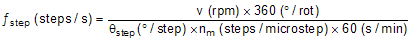
θstep can be found in the stepper motor data sheet or written on the motor itself.

The frequency ƒstep gives the frequency of input change on the device. For the design parameters mentioned above, fstep can be calculated as 800 Hz.

Equation 3. GUID-A1D03E41-3BFD-4B68-B914-D789430C133D-low.gif