SLOS709C June   2011  – December 2022 DRV8662

PRODUCTION DATA  

  1. Features
  2. Applications
  3. Description
  4. Revision History
  5. Pin Configuration and Functions
  6. Specifications
    1. 6.1 Absolute Maximum Ratings
    2. 6.2 ESD Ratings
    3. 6.3 Recommended Operating Conditions
    4. 6.4 Thermal Information
    5. 6.5 Electrical Characteristics
    6. 6.6 Timing Requirements
    7. 6.7 Typical Characteristics
  7. Detailed Description
    1. 7.1 Overview
    2. 7.2 Functional Block Diagram
    3. 7.3 Feature Description
      1. 7.3.1 Fast Start-up (Enable Pin)
      2. 7.3.2 Gain Control
      3. 7.3.3 Adjustable Boost Voltage
      4. 7.3.4 Adjustable Boost Current Limit
      5. 7.3.5 Internal Charge Pump
      6. 7.3.6 Thermal Shutdown
    4. 7.4 Device Functional Modes
      1. 7.4.1 Startup/shutdown Sequencing
        1. 7.4.1.1 PWM Source
        2. 7.4.1.2 DAC Source
      2. 7.4.2 Low-voltage Operation
    5. 7.5 Programming
      1. 7.5.1 Programming the Boost Voltage
      2. 7.5.2 Programing the Boost Current Limit
  8. Application and Implementation
    1. 8.1 Application Information
    2. 8.2 Typical Application
      1. 8.2.1 DRV8662 System Diagram with DAC Input
        1. 8.2.1.1 Design Requirements
        2. 8.2.1.2 Detailed Design Procedure
          1. 8.2.1.2.1 Inductor Selection
          2. 8.2.1.2.2 Piezo Actuator Selection
          3. 8.2.1.2.3 Boost Capacitor Selection
          4. 8.2.1.2.4 Current Consumption Calculation
          5. 8.2.1.2.5 Input Filter Considerations
        3. 8.2.1.3 Application Curves
      2. 8.2.2 DRV8662 System Diagram with Filtered Single-Ended PWM Input
        1. 8.2.2.1 Design Requirements
        2. 8.2.2.2 Detailed Design Procedure
          1. 8.2.2.2.1 Input Filter Design
        3. 8.2.2.3 Application Curves
  9. Power Supply Recommendations
  10. 10Layout
    1. 10.1 Layout Guidelines
    2. 10.2 Layout Example
  11. 11Device and Documentation Support
    1. 11.1 Documentation Support
      1. 11.1.1 Related Documentation
    2. 11.2 Trademarks
  12. 12Mechanical, Packaging, and Orderable Information

Package Options

Mechanical Data (Package|Pins)
Thermal pad, mechanical data (Package|Pins)
Orderable Information

Programming the Boost Voltage

The boost output voltage (VBST) is programmed via two external resistors as shown in Figure 7-1.

GUID-A7D10AA9-C6D9-4931-B6F6-BCDFE12D3BD6-low.gifFigure 7-1 Boost Voltage Programming

The boost output voltage is given by Equation 1:
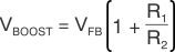
Equation 1. GUID-B4818394-7D74-4D5E-88A4-EDDCBCE4380C-low.gif

where VFB = 1.32 V.

VBST should be programmed to a value 5.0 V greater than the largest peak voltage expected in the system to allow adequate amplifier headroom. Since the programming range for the boost voltage extends to 105 V, the leakage current through the resistor divider can become significant. It is recommended that the sum of the resistance of R1 and R2 be greater than 500 kΩ. Note that when resistor values greater than 1 MΩ are used, PCB contamination may cause boost voltage inaccuracy. Exercise caution when soldering large resistances, and clean the area when finished for best results.