SLVS857B December 2009 – January 2015 DRV8808
PRODUCTION DATA.
- 1 Features
- 2 Applications
- 3 Description
- 4 Revision History
- 5 Pin Configuration and Functions
- 6 Specifications
-
7 Detailed Description
- 7.1 Overview
- 7.2 Functional Block Diagram
- 7.3
Feature Description
- 7.3.1
Setup Mode, Extended Setup Mode, Power-Down Mode
- 7.3.1.1 Operation Setup Register Bit Assignment
- 7.3.1.2 Operation Extended Setup Register Bit Assignment
- 7.3.1.3 Deep Sleep Mode
- 7.3.1.4 DC Motor Drive
- 7.3.1.5 Short/Open for Motor Outputs
- 7.3.1.6 Charge Pump
- 7.3.1.7 DC-DC Converters
- 7.3.1.8 nReset: Input for System Reset
- 7.3.1.9 VM Start-up/Power-Down and Glitch Condition
- 7.3.2 Blanking Time Insertion Timing for DC Motor Driving
- 7.3.3 Function Table in nORT, Power Down, VM Conditions
- 7.3.1
Setup Mode, Extended Setup Mode, Power-Down Mode
- 7.4 Device Functional Modes
- 7.5 Programming
- 8 Application and Implementation
- 9 Power Supply Recommendations
- 10Layout
- 11Device and Documentation Support
- 12Mechanical, Packaging, and Orderable Information
Package Options
Mechanical Data (Package|Pins)
- DCA|48
Thermal pad, mechanical data (Package|Pins)
- DCA|48
Orderable Information
8 Application and Implementation
NOTE
Information in the following applications sections is not part of the TI component specification, and TI does not warrant its accuracy or completeness. TI’s customers are responsible for determining suitability of components for their purposes. Customers should validate and test their design implementation to confirm system functionality.
8.1 Application Information
The DRV8808 provides an integrated motor driver solution. The chip has three H-bridges internally and is configurable to different settings by SPI communication.
8.2 Typical Application
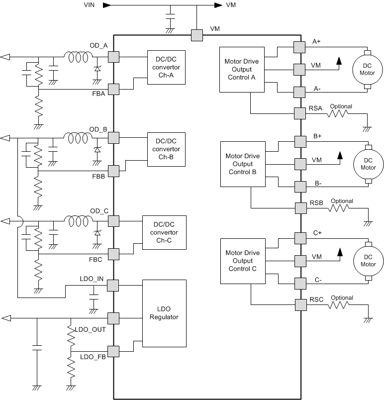 Figure 27. 3 DC Motors, 3 Switching Regulators and 1 LDO Usage Case
8.2.1 Design Requirements
To begin the design process, determine the following:
- Output voltage for each DC-DC converter and LDO.
- Output voltage start up sequence.
- Other parameters through SPI.
8.2.2 Detailed Design Procedure
8.2.2.1 Output Voltage for Each DC-DC Converter
Output voltage is set by external feedback resister network. For example,
1.5-V Output : 1.0 KΩ and 2.0 KΩ
1.0-V Output : 0 Ω and 3.0 KΩ
3.3-V Output : 6.8 KΩ and 1.5 KΩ
8.2.2.2 Output Voltage Start Up Sequence
DC-DC converters start up sequence is determined by CSELECT pin. See DC-DC Converters for details.
8.2.2.3 Other Parameters
Other parameters are programmed through SPI.
8.2.2.4 Motor Configuration
Many parameters are set by SPI register setting. Ramp up device with nSLEEP = Low, then write setup registers through SPI.
8.2.3 Application Curves
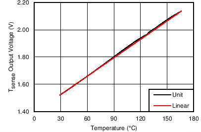 Figure 28. Tsense (Analog Out) Temperate Coefficient: Voltage Plot Example (Typical)
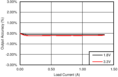 Figure 29. DC-DC Converter - DC Load Regulation Example (Typical)