SNLS561B February 2017 – October 2019 DS250DF210
PRODUCTION DATA.
- 1 Features
- 2 Applications
- 3 Description
- 4 Revision History
- 5 Description (continued)
- 6 Pin Configuration and Functions
-
7 Specifications
- 7.1 Absolute Maximum Ratings
- 7.2 ESD Ratings
- 7.3 Recommended Operating Conditions
- 7.4 Thermal Information
- 7.5 Electrical Characteristics
- 7.6 Timing Requirements, Retimer Jitter Specifications
- 7.7 Timing Requirements, Retimer Specifications
- 7.8 Timing Requirements, Recommended Calibration Clock Specifications
- 7.9 Recommended SMBus Switching Characteristics (Slave Mode)
- 7.10 Recommended SMBus Switching Characteristics (Master Mode)
- 7.11 Typical Characteristics
-
8 Detailed Description
- 8.1 Overview
- 8.2 Functional Block Diagram
- 8.3
Feature Description
- 8.3.1 Device Data Path Operation
- 8.3.2 Signal Detect
- 8.3.3 Continuous Time Linear Equalizer (CTLE)
- 8.3.4 Variable Gain Amplifier (VGA)
- 8.3.5 Cross-Point Switch
- 8.3.6 Decision Feedback Equalizer (DFE)
- 8.3.7 Clock and Data Recovery (CDR)
- 8.3.8 Calibration Clock
- 8.3.9 Differential Driver With FIR Filter
- 8.3.10 Debug Features
- 8.3.11 Interrupt Signals
- 8.4 Device Functional Modes
- 8.5 Programming
- 8.6 Register Maps
- 9 Application and Implementation
- 10Power Supply Recommendations
- 11Layout
- 12Device and Documentation Support
- 13Mechanical, Packaging, and Orderable Information
Package Options
Mechanical Data (Package|Pins)
- ABM|101
Thermal pad, mechanical data (Package|Pins)
Orderable Information
11.2 Layout Example
The following example layout demonstrates how all signals can be escaped from the BGA array using stripline routing on a generic 28-layer stackup. This example layout assumes the following:
- Trace width: 0.159 mm (6.25 mil)
- Trace edge-to-edge spacing: 0.197 mm (7.75 mil)
- VIA-to-VIA spacing: 0.7 mm (27.9 mil) minimum; Note: 1.0 mm VIA-to-VIA spacing is also achievable if PCB manufacturing rules stipulate
- No VIA-in-pad used
NOTE
Some TI test pins (that is, NC_TEST[5:0]) are routed in this example layout, but in most applications these pins can be left floating.
Many other escape routing options exist using different trace width and spacing combinations. The optimum trace width and spacing depend on the PCB material, PCB routing density, and other factors.
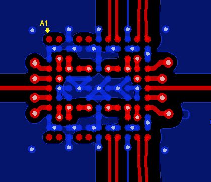 Figure 24. Top Layer (Pin A1 is Top-Left)
 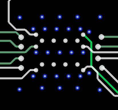 Figure 26. Internal Low-Speed Signal Layers (Pin A1 is Top-Left)
 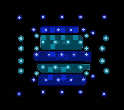 Figure 28. Bottom Layer (Pin A1 is Top-Left)
 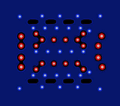 Figure 25. Layer 1 GND (Pin A1 is Top-Left)
 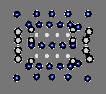 Figure 27. VDD Layer (Pin A1 is Top-Left)