SNLS244H September 2006 – January 2016 DS42MB100
PRODUCTION DATA.
- 1 Features
- 2 Applications
- 3 Description
- 4 Revision History
- 5 Pin Configuration and Functions
- 6 Specifications
- 7 Parameter Measurement Information
- 8 Detailed Description
- 9 Application and Implementation
- 10Power Supply Recommendations
- 11Layout
- 12Device and Documentation Support
- 13Mechanical, Packaging, and Orderable Information
Package Options
Refer to the PDF data sheet for device specific package drawings
Mechanical Data (Package|Pins)
- NJK|36
Thermal pad, mechanical data (Package|Pins)
Orderable Information
9 Application and Implementation
NOTE
Information in the following applications sections is not part of the TI component specification, and TI does not warrant its accuracy or completeness. TI’s customers are responsible for determining suitability of components for their purposes. Customers should validate and test their design implementation to confirm system functionality.
9.1 Application Information
The DS42MB100 is a 2:1 MUX and 1:2 buffer that equalizes input data up to 4.25 Gbps and provides transmit pre-emphasis controls to improve overall signal reach. As a MUX buffer, the DS42MB100 is ideal for designs where there is a need for port sharing or redundancy as well as on-the-fly reorganization of routes and data connections.
9.2 Typical Application
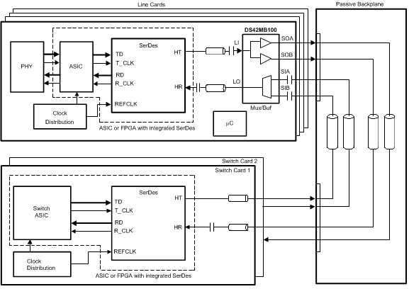
A typical application for the DS42MB100 is shown in Figure 10 and Figure 11.
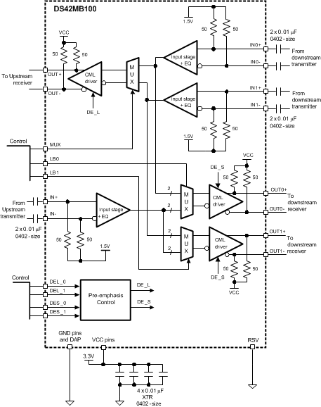 Figure 11. DS42MB100 Connection Block Diagram
9.2.1 Design Requirements
In a typical design, the DS42MB100 equalizes a short backplane trace on its input, followed by a longer trace at the DS42MB100 output. In this application example, a 25-inch FR4 coupled micro-strip board trace is used in place of the short backplane link. A block diagram of this example is shown in Figure 12.
 Figure 12. Block Diagram of DS42MB100 Application Example
The 25-inch microstrip board trace has approximately 6 dB of attenuation between 375 MHz and 1.875 GHz, representing closely the transmission loss of the short backplane transmission line. The 25-inch microstrip is connected between the pattern generator and the differential inputs of the DS42MB100 for AC measurements.
Table 6. Input Trace Parameters
| TRACE LENGTH | FINISHED TRACE WIDTH W | SEPARATION BETWEEN TRACES | DIELECTRIC HEIGHT H | DIELECTRIC CONSTANT εR | LOSS TANGENT |
|---|---|---|---|---|---|
| 25 inches | 8.5 mil | 11.5 mil | 6 mil | 3.8 | 0.022 |
The length of the output trace may vary based on system requirements. In this example, a 40-inch FR4 trace with similar trace width, separation, and dielectric characteristics, is placed at the DS42MB100 output.
As with any high speed design, there are many factors which influence the overall performance. Following is a list of critical areas for consideration and study during design.
- Use 100-Ω impedance traces. Generally these are very loosely coupled to ease routing length differences.
- Place AC-coupling capacitors near to the receiver end of each channel segment to minimize reflections.
- The maximum body size for AC-coupling capacitors is 0402.
- Back-drill connector vias and signal vias to minimize stub length.
- Use reference plane vias to ensure a low inductance path for the return current.
9.2.2 Detailed Design Procedure
For optimal design, the DS42MB100 must be configured to route incoming data correctly as well as provide the best signal quality. The following design procedures should be observed:
- The DS42MB100 should be configured to provide the correct MUX and buffer routes in order to satisfy system requirements. In order to set the appropriate MUX control settings, refer to Table 2. To configure the buffer control settings, refer to Table 3. For example, consider the case where the designer wishes to route the input from Switch Card 0 (IN0±) to the output for the line card (OUT±). To accomplish this, set MUX = 1 (select IN0±). For the other direction from line card output to switch card, set LB0 = 1 and LB1 = 1 so that the input from the line card is buffered to both Switch Card 0 (OUT0±) and Switch Card 1 (OUT1±).
- The DS42MB100 is designed to be placed at an offset location with respect to the overall channel attenuation. To optimize performance, determine whether input and output equalization is required. Set EQL = 0 and EQS = 0 to enable input equalization. The MUX buffer transmit pre-emphasis can be tuned to extend the trace length reach while also recovering a solid eye opening. To tune transmit pre-emphasis on either the line card side or switch card side, refer to Table 4 and Table 5 for recommended pre-emphasis control settings according to the length of FR4 board trace connected at the DS42MB100 output. For example, if 40 inches of FR4 trace is connected to the switch card output, set DES_[1:0] = (1, 1) for VOD = 1200 mVpp and –9 dB of transmit pre-emphasis.
9.2.3 Application Curves
Figure 13 through Figure 18 show how the signal integrity varies at different places in the data path. These measured locations can be referenced back to the labeled points provided in Figure 12.
- Point (A): Output signal of source pattern generator
- Point (B): Input to DS42MB100 after 25 inches of FR4 trace from source
- Point (C): Output of DS42MB100 driver
- Point (D): Signal after 40 inches of FR4 trace from DS42MB100 driver
The source signal is a PRBS-7 pattern at 4 Gbps. For the long output traces, the eye after 40 inches of output FR4 trace is significantly improved by adding –9 dB of pre-emphasis.
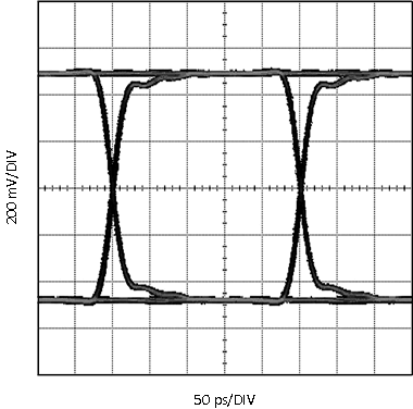 Figure 13. Eye Measured at Point (A)
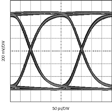 Figure 15. Eye Measured at Point (C),
 Pre-Emphasis = 0 dB
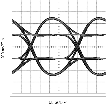 Figure 17. Eye Measured at Point (C),
 Pre-Emphasis = –9 dB
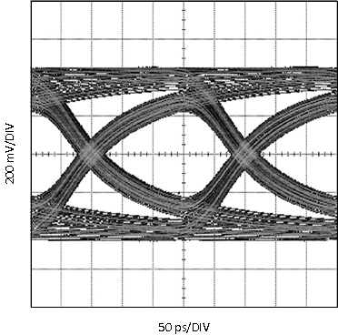 Figure 14. Eye Measured at Point (B)
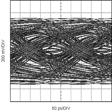 Figure 16. Eye Measured at Point (D),
 Pre-Emphasis = 0 dB
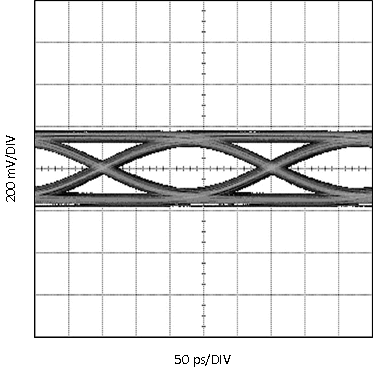 Figure 18. Eye Measured at Point (D),
 Pre-Emphasis = –9 dB
