SNLS334G April 2011 – January 2015 DS80PCI800
PRODUCTION DATA.
- 1 Features
- 2 Applications
- 3 Description
- 4 Revision History
- 5 Pin Configuration and Functions
- 6 Specifications
- 7 Parameter Measurement Information
- 8 Detailed Description
- 9 Application and Implementation
- 10Power Supply Recommendations
- 11Layout
- 12Device and Documentation Support
- 13Mechanical, Packaging, and Orderable Information
Package Options
Mechanical Data (Package|Pins)
- NJY|54
Thermal pad, mechanical data (Package|Pins)
Orderable Information
10 Power Supply Recommendations
10.1 3.3-V or 2.5-V Supply Mode Operation
The DS80PCI800 has an optional internal voltage regulator to provide the 2.5 V supply to the device. In 3.3-V mode, the VIN pin = 3.3 V is used to supply power to the device and the VDD pins should be left open. The internal regulator will provide the 2.5 V to the VDD pins of the device and a 0.1 μF cap is needed at each of the five VDD pins for power supply de-coupling (total capacitance should be ≤ 0.5 µF), and the VDD pins should be left open. The VDD_SEL pin must be tied to GND to enable the internal regulator. In 2.5-V mode, the VIN pin should be left open and 2.5 V supply must be applied to the VDD pins. The VDD_SEL pin must be left open (no connect) to disable the internal regulator.
The DS80PCI800 can be configured for 2.5 V operation or 3.3 V operation. The lists below outline required connections for each supply selection.
3.3-V Mode of Operation
- Tie VDD_SEL = 0 with 1-kΩ resistor to GND.
- Feed 3.3-V supply into VIN pin. Local 1.0-µF decoupling at VIN is recommended.
- See information on VDD bypass below.
- SDA and SCL pins should connect pullup resistor to VIN
- Any 4-Level input which requires a connection to "Logic 1" should use a 1-kΩ resistor to VIN
2.5-V Mode of Operation
- VDD_SEL = Float
- VIN = Float
- Feed 2.5-V supply into VDD pins.
- See information on VDD bypass below.
- SDA and SCL pins connect pullup resistor to VDD for 2.5-V uC SMBus IO
- SDA and SCL pins connect pullup resistor to VDD for 3.3-V uC SMBus IO
- Any 4-Level input which requires a connection to "Logic 1" should use a 1-kΩ resistor to VIN
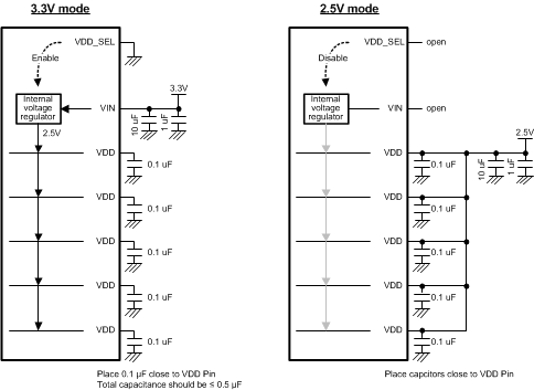 Figure 14. 3.3 V or 2.5 V Supply Connection Diagram
10.2 Power Supply Bypassing
Two approaches are recommended to ensure that the DS80PCI800 is provided with an adequate power supply bypass. First, the supply (VDD) and ground (GND) pins should be connected to power planes routed on adjacent layers of the printed circuit board. Second, careful attention to supply bypassing through the proper use of bypass capacitors is required. A 0.1-μF bypass capacitor should be connected to each VDD pin such that the capacitor is placed as close as possible to the device. Small body size capacitors (such as 0402) reduce the parasitic inductance of the capacitor and also help in placement close to the VDD pin. If possible, the layer thickness of the dielectric should be minimized so that the VDD and GND planes create a low inductance supply with distributed capacitance.