SNLS416D June 2012 – January 2015 DS90UB927Q-Q1
PRODUCTION DATA.
- 1 Features
- 2 Applications
- 3 Description
- 4 Revision History
- 5 Pin Configuration and Functions
-
6 Specifications
- 6.1 Absolute Maximum Ratings
- 6.2 ESD Ratings
- 6.3 Recommended Operating Conditions
- 6.4 Thermal Information
- 6.5 DC Electrical Characteristics
- 6.6 AC Electrical Characteristics
- 6.7 Electrical Characteristics: DC and AC Serial Control Bus
- 6.8 Timing Requirements for the Serial Control Bus
- 6.9 Timing Requirements - DC and AC Serial Control Bus Characteristics
- 6.10 Typical Characteristics
-
7 Detailed Description
- 7.1 Overview
- 7.2 Functional Block Diagram
- 7.3
Feature Description
- 7.3.1 High-Speed Forward Channel Data Transfer
- 7.3.2 Low-Speed Back Channel Data Transfer
- 7.3.3 Common Mode Filter Pin (CMF)
- 7.3.4 Video Control Signals
- 7.3.5 EMI Reduction Features
- 7.3.6 Built-In Self Test (BIST)
- 7.3.7 Forward Channel and Back Channel Error Checking
- 7.3.8 Internal Pattern Generation
- 7.3.9 Remote Auto Power-Down Mode
- 7.3.10 Input RxCLKIN Loss Detect
- 7.3.11 Serial Link Fault Detect
- 7.3.12 Interrupt Pin (INTB)
- 7.3.13 General-Purpose I/O
- 7.3.14 I2S Audio Interface
- 7.3.15 Additional Features
- 7.4 Device Functional Modes
- 7.5 Programming
- 7.6 Register Maps
- 8 Application and Implementation
- 9 Power Supply Recommendations
- 10Layout
- 11Device and Documentation Support
- 12Mechanical, Packaging, and Orderable Information
Package Options
Refer to the PDF data sheet for device specific package drawings
Mechanical Data (Package|Pins)
- RTA|40
Thermal pad, mechanical data (Package|Pins)
- RTA|40
Orderable Information
10 Layout
10.1 Layout Guidelines
Circuit board layout and stack-up for the LVDS serializer and deserializer devices should be designed to provide low-noise power to the device. Good layout practice will also separate high frequency or high-level inputs and outputs to minimize unwanted stray noise, feedback and interference. Power system performance may be greatly improved by using thin dielectrics (2 to 4 mil) for power / ground sandwiches. This arrangement utilizes the plane capacitance for the PCB power system and has low-inductance, which has proven effectiveness especially at high frequencies, and makes the value and placement of external bypass capacitors less critical. External bypass capacitors should include both RF ceramic and tantalum electrolytic types. RF capacitors may use values in the range of 0.01 μF to 10 μF. Tantalum capacitors may be in the 2.2 μF to 10 μF range. The voltage rating of the tantalum capacitors should be at least 5X the power supply voltage being used.
MLCC surface mount capacitors are recommended due to their smaller parasitic properties. When using multiple capacitors per supply pin, locate the smaller value closer to the pin. A large bulk capacitor is recommended at the point of power entry. This is typically in the 50 μF to 100 μF range and will smooth low frequency switching noise. It is recommended to connect power and ground pins directly to the power and ground planes with bypass capacitors connected to the plane with via on both ends of the capacitor. Connecting power or ground pins to an external bypass capacitor will increase the inductance of the path. A small body size X7R chip capacitor, such as 0603 or 0805, is recommended for external bypass. A small body sized capacitor has less inductance. The user must pay attention to the resonance frequency of these external bypass capacitors, usually in the range of 20 MHz to 30 MHz. To provide effective bypassing, multiple capacitors are often used to achieve low impedance between the supply rails over the frequency of interest. At high frequency, it is also a common practice to use two vias from power and ground pins to the planes, reducing the impedance at high frequency.
Some devices provide separate power and ground pins for different portions of the circuit. This is done to isolate switching noise effects between different sections of the circuit. Separate planes on the PCB are typically not required. Pin Description tables typically provide guidance on which circuit blocks are connected to which power pin pairs. In some cases, an external filter may be used to provide clean power to sensitive circuits such as PLLs. For DS90UB927Q-Q1, only one common ground plane is required to connect all device related ground pins.
Use at least a four layer board with a power and ground plane. Locate LVCMOS signals away from the LVDS lines to prevent coupling from the LVCMOS lines to the LVDS lines. Closely coupled differential lines of 100Ω are typically recommended for LVDS interconnect. The closely coupled lines help to ensure that coupled noise will appear as common mode and thus is rejected by the receivers. The tightly coupled lines will also radiate less.
At least 9 thermal vias are necessary from the device center DAP to the ground plane. They connect the device ground to the PCB ground plane, as well as conduct heat from the exposed pad of the package to the PCB ground plane. More information on the WQFN style package, including PCB design and manufacturing requirements, is provided in TI Application Note: AN-1187 Leadless Leadframe Package (LLP) (SNOA401).
10.1.1 CML Interconnect Guidelines
See SNLA008 and SNLA035 for full details.
- Use 100-Ω coupled differential pairs
- Use the S/2S/3S rule in spacings
- – S = space between the pair
- – 2S = space between pairs
- – 3S = space to LVCMOS signal
- Minimize the number of Vias
- Use differential connectors when operating above 500 Mbps line speed
- Maintain balance of the traces
- Minimize skew within the pair
- Terminate as close to the TX outputs and RX inputs as possible.
Additional general guidance can be found in the LVDS Owner’s Manual - available at: SNLA187
10.2 Layout Example
Figure 34 PCB layout example is derived from the layout design of the DS90UB927Q-Q1 Evaluation Board. The graphic and layout description are used to determine both proper routing and proper solder techniques when designing the Serializer board.
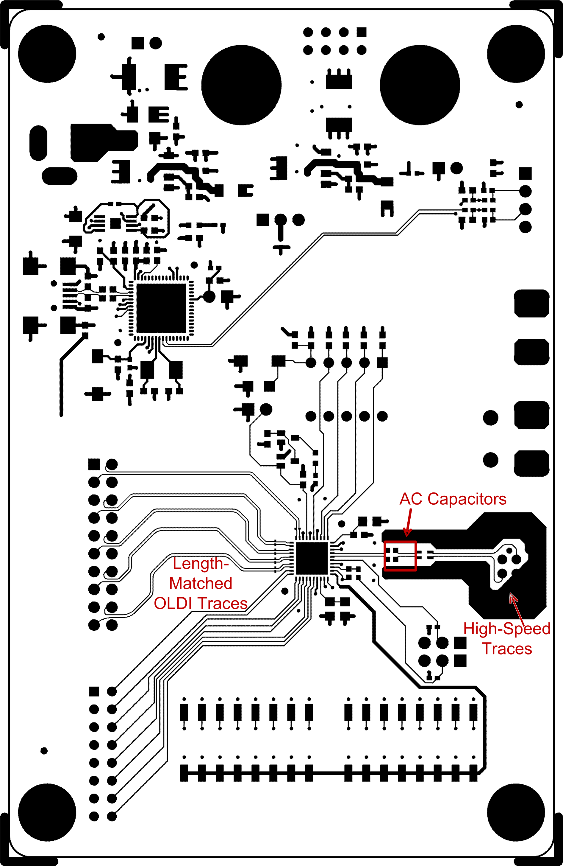 Figure 34. DS90UB927Q-Q1 Serializer Example Layout