SNLS302E May 2010 – February 2015 DS92LV2411 , DS92LV2412
PRODUCTION DATA.
- 1 Features
- 2 Applications
- 3 Description
- 4 Revision History
- 5 Pin Configuration and Functions
-
6 Specifications
- 6.1 Absolute Maximum Ratings
- 6.2 ESD Ratings
- 6.3 Recommended Operating Conditions
- 6.4 Thermal Information
- 6.5 Serializer DC Electrical Characteristics
- 6.6 Deserializer DC Electrical Characteristics
- 6.7 DC and AC Serial Control Bus Characteristics
- 6.8 Recommended Timing For The Serial Control Bus
- 6.9 Recommended Serializer Timing For CLKIN
- 6.10 Serializer Switching Characteristics
- 6.11 Deserializer Switching Characteristics
- 6.12 Typical Characteristics
-
7 Detailed Description
- 7.1 Overview
- 7.2 Functional Block Diagrams
- 7.3
Feature Description
- 7.3.1 Serializer Functional Description
- 7.3.2
Deserializer Functional Description
- 7.3.2.1 Integrated Signal Conditioning Features — Des
- 7.3.2.2 EMI Reduction Features
- 7.3.2.3 Power Saving Features
- 7.3.2.4 Des — Clock-Data Recovery Status Flag (Lock) And Output State Select (OSS_SEL)
- 7.3.2.5 Des — Oscillator Output — Optional
- 7.3.2.6 Des — OP_LOW — Optional
- 7.3.2.7 Des — Clock Edge Select (RFB)
- 7.3.2.8 Des — Control Signal Filter — Optional
- 7.3.2.9 Des — SSCG Low Frequency Optimization (Lf_mode)
- 7.3.2.10 Des — Strap Input Pins
- 7.3.3 Built In Self Test (BIST)
- 7.4 Device Functional Modes
- 7.5 Programming
- 7.6 Register Maps
- 8 Applications and Implementation
- 9 Power Supply Recommendations
- 10Layout
- 11Device and Documentation Support
- 12Mechanical, Packaging, and Orderable Information
Package Options
Mechanical Data (Package|Pins)
- NKB|60
Thermal pad, mechanical data (Package|Pins)
Orderable Information
10 Layout
10.1 Layout Guidelines
Circuit board layout and stack-up for the Ser/Des devices should be designed to provide low-noise power feed to the device. Good layout practice will also separate high frequency or high-level inputs and outputs to minimize unwanted stray noise pickup, feedback and interference. Power system performance may be greatly improved by using thin dielectrics (2 to 4 mils) for power / ground sandwiches. This arrangement provides plane capacitance for the PCB power system with low-inductance parasitics, which has proven especially effective at high frequencies, and makes the value and placement of external bypass capacitors less critical. External bypass capacitors should include both RF ceramic and tantalum electrolytic types. RF capacitors may use values in the range of 0.01 uF to 0.1 uF. Tantalum capacitors may be in the 2.2 uF to 10 uF range. Voltage rating of the tantalum capacitors should be at least 5X the power supply voltage being used.
Surface mount capacitors are recommended due to their smaller parasitics. When using multiple capacitors per supply Pin, locate the smaller value closer to the Pin. A large bulk capacitor is recommend at the point of power entry. This is typically in the 50uF to 100uF range and will smooth low frequency switching noise. It is recommended to connect power and ground Pins directly to the power and ground planes with bypass capacitors connected to the plane with via on both ends of the capacitor. Connecting power or ground Pins to an external bypass capacitor will increase the inductance of the path.
A small body size X7R chip capacitor, such as 0603, is recommended for external bypass. Its small body size reduces the parasitic inductance of the capacitor. The user must pay attention to the resonance frequency of these external bypass capacitors, usually in the range of 20-30 MHz. To provide effective bypassing, multiple capacitors are often used to achieve low impedance between the supply rails over the frequency of interest. At high frequency, it is also a common practice to use two vias from power and ground Pins to the planes, reducing the impedance at high frequency.
Use at least a four layer board with a power and ground plane. Locate LVCMOS signals away from the CML lines to prevent coupling from the LVCMOS lines to the CML lines. Closely-coupled differential lines of 100 Ohms are typically recommended for differential interconnect. The closely coupled lines help to ensure that coupled noise will appear as common-mode and thus is rejected by the receivers. The tightly coupled lines will also radiate less.
Information on the WQFN style package is provided in TI Application Note: AN-1187 (SNOA401).
10.2 Layout Example
Stencil parameters such as aperture area ratio and the fabrication process have a significant impact on paste deposition. Inspection of the stencil prior to placement of the LLP package is highly recommended to improve board assembly yields. If the via and aperture openings are not carefully monitored, the solder may flow unevenly through the DAP. Stencil parameters for aperture opening and via locations are shown below:
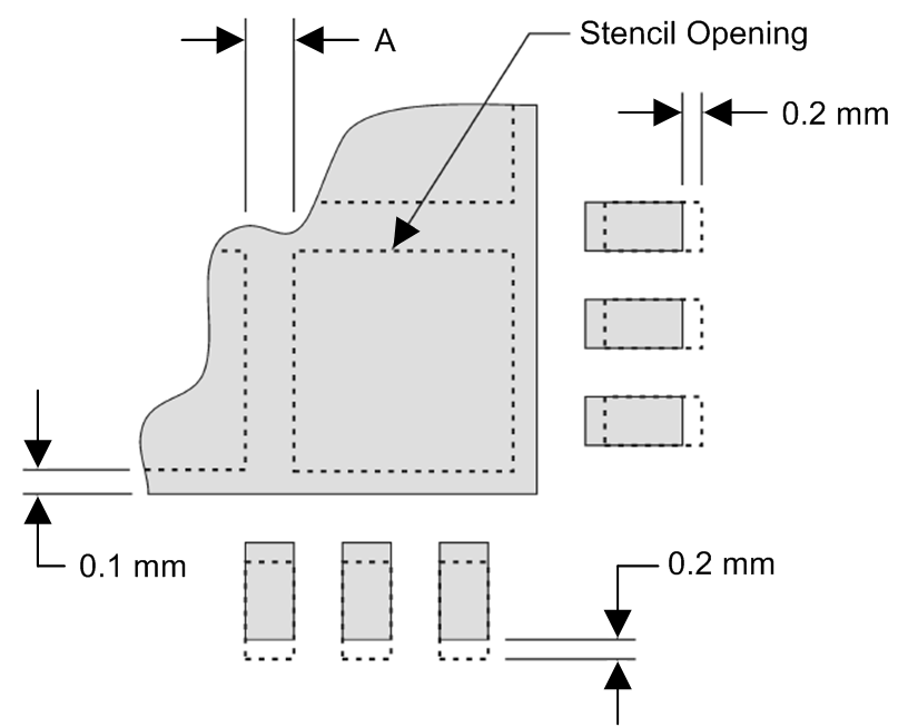 Figure 39. No Pullback LLP, Single Row Reference Diagram
Table 16. No Pullback LLP Stencil Aperture Summary for DS92LV2411 and DS92LV2412
| Device | Pin Count | MKT Dwg | PCB I/O Pad Size (mm) | PCB Pitch (mm) | PCB DAP size (mm) | Stencil I/O Aperture (mm) | Stencil DAP Aperture (mm) | Number of DAP Aperture Openings | Gap Between DAP Aperture (Dim A mm) |
|---|---|---|---|---|---|---|---|---|---|
| DS92LV2411 | 48 | SQA48A | 0.25 x 0.6 | 0.5 | 5.1 x 5.1 | 0.25 x 0.7 | 1.1 x 1.1 | 16 | 0.2 |
| DS92LV2412 | 60 | SQA60B | 0.25 x 0.8 | 0.5 | 7.2 x 7.2 | 0.25 x 0.9 | 1.16 x 1.16 | 25 | 0.3 |
 Figure 40. 48-Pin WQFN Stencil Example of Via and Opening Placement
The following PCB layout examples are derived from the layout design of the DS9LV2411 and DS92LV2412 in the LV24EVK01 Evaluation Module User's Guide (SNLU006). These graphics and additional layout description are used to demonstrate both proper routing and proper solder techniques when designing in the Ser/Des pair.
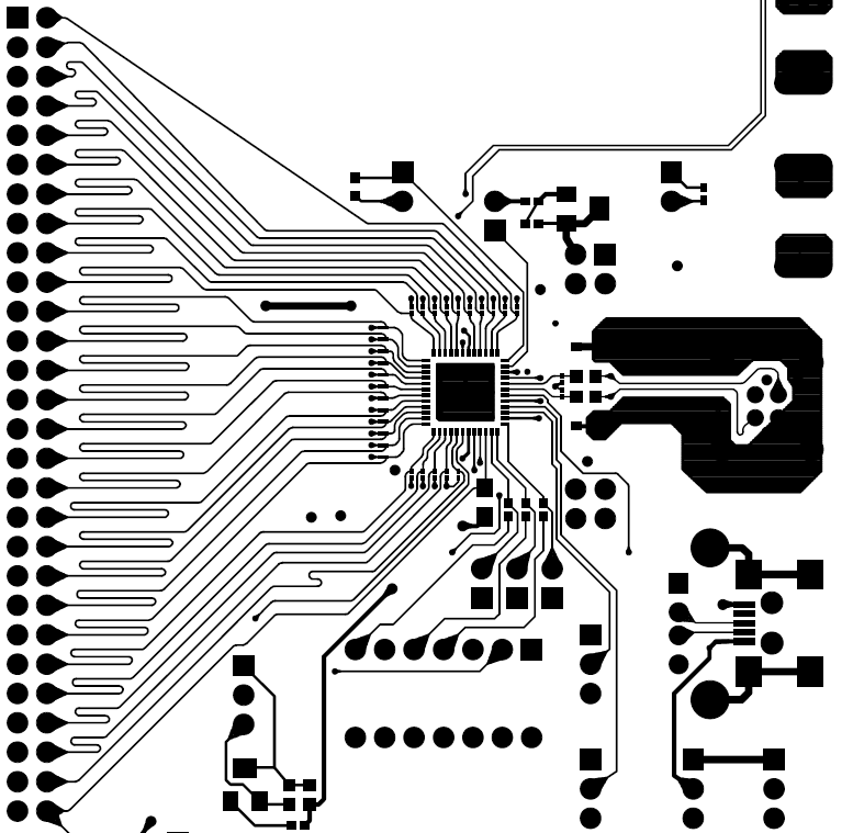 Figure 41. DS92LV2411 Serializer Example Layout
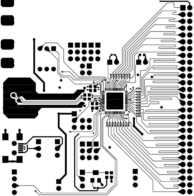 Figure 42. DS92LV2412 Deserializer Example Layout