SNLS582C June 2017 – September 2020 FPC402
PRODUCTION DATA
- 1 Features
- 2 Applications
- 3 Description
- 4 Revision History
- 5 Description (continued)
- 6 Pin Configuration and Functions
- 7 Specifications
-
8 Detailed Description
- 8.1 Overview
- 8.2 Functional Block Diagram
- 8.3
Feature Description
- 8.3.1 Host-Side Control Interface
- 8.3.2 LED Control
- 8.3.3 Low-Speed Output Signal Control
- 8.3.4 Low-Speed Input Status and Interrupt Generation
- 8.3.5 Downstream (Port-Side) I2C Master
- 8.3.6 Data Prefetch From Modules
- 8.3.7 Scheduled Write
- 8.3.8 Protocol Timeouts
- 8.3.9 General-Purpose Inputs and Outputs
- 8.3.10 Hot-Plug Support
- 8.4 Device Functional Modes
- 8.5 Programming
- 9 Application and Implementation
- 10Power Supply Recommendations
- 11Layout
- 12Device and Documentation Support
- 13Mechanical, Packaging, and Orderable Information
Package Options
Mechanical Data (Package|Pins)
- RHU|56
Thermal pad, mechanical data (Package|Pins)
Orderable Information
3 Description
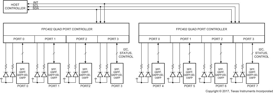
The FPC402 quad port controller serves as a low-speed signal aggregator for common port types such as SFP, QSFP, Mini-SAS HD, and others. The FPC402 aggregates all low-speed control and I2C signals across four ports and presents a single easy-to-use management interface to the host (I2C or SPI). Multiple FPC402s can be used in high-port-count applications with one common control interface to the host. The FPC402 is designed to allow placement on the bottom side of the PCB, underneath the press fit connector, to simplify routing. This localized control of the low-speed signals in the ports cuts system BOM costs by enabling the use of smaller IO count control devices (FPGAs, CPLDs, and MCUs) and by reducing routing layer congestion.
| PART NUMBER | PACKAGE | BODY SIZE (NOM) |
|---|---|---|
| FPC402 | WQFN (56) | 5.00 mm × 11.00 mm |
| PART NUMBER | ACCESSIBLE DOWNSTREAM ADDRESSES | PIN COMPATIBLE |
|---|---|---|
| FPC402 | All valid I2C addreses | Yes |
| FPC401 | MSA Addresses: 0xA0, 0xA2 | Yes |
 Simplified Block Diagram