SLAS971E May 2014 – December 2020 HD3SS215
PRODUCTION DATA
- 1 Features
- 2 Applications
- 3 Description
- 4 Revision History
- 5 Description (continued)
- 6 Pin Configuration and Functions
- 7 Specifications
- 8 Detailed Description
- 9 Applications and Implementation
- 10Layout
- 11Device and Documentation Support
- 12Mechanical, Packaging, and Orderable Information
Package Options
Mechanical Data (Package|Pins)
Thermal pad, mechanical data (Package|Pins)
- RTQ|56
Orderable Information
9.2.1 DisplayPort and Dual Mode Adapter with Two Sources
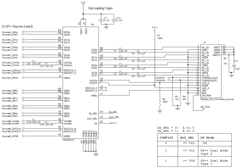
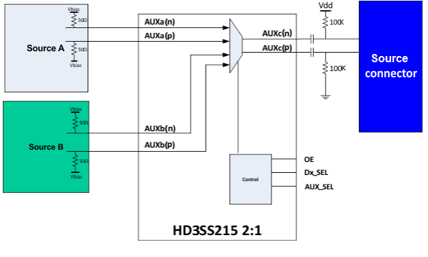
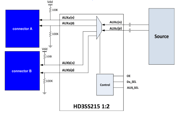
The application schematic below shows the HD3SS215 in the 2:1 configuration for DisplayPort switching. The HD3SS215 receives inputs from DP Source A and DP Source B. The control pins of the device can be set to select Source A/B inputs and transfer them to port C through the Dx_SEL control pin. The schematic also shows the CONFIG1 and AUX_SEL settings to configure the HD3SS215 to work with DP++ Type 2 and Type1 adapters. For this specific schematic, the AC capacitors needed on the MainLink signal lines are shown on the Sink side of the HD3SS215. This is done to decrease the BOM. If desired the AC capacitors maybe placed in the signal path on the Source A/B side of HD3SS215. Additional diagrams are provided to show the configuration of the AUX channel for 2:1 and 1:2 DisplayPort only applications.
 Figure 9-1 HD3SS215 Application Diagram for DisplayPort or Dual Mode Adapter Configuration
 Figure 9-2 HD3SS215 AUX Channel in 2:1 DisplayPort Application
 Figure 9-3 HD3SS215 AUX Channel in 1:2 DisplayPort Application