SLAS974 December 2017 HD3SS3412A
PRODUCTION DATA.
- 1 Features
- 2 Applications
- 3 Description
- 4 Revision History
- 5 Description (continued)
- 6 Pin Configuration and Functions
- 7 Specifications
- 8 Parameter Measurement Information
- 9 Detailed Description
- 10Application and Implementation
- 11Power Supply Recommendations
- 12Layout
- 13Device and Documentation Support
- 14Mechanical, Packaging, and Orderable Information
Package Options
Mechanical Data (Package|Pins)
- RUA|42
Thermal pad, mechanical data (Package|Pins)
- RUA|42
Orderable Information
10 Application and Implementation
NOTE
Information in the following applications sections is not part of the TI component specification, and TI does not warrant its accuracy or completeness. TI’s customers are responsible for determining suitability of components for their purposes. Customers should validate and test their design implementation to confirm system functionality.
10.1 Application Information
10.1.1 AC Coupling Caps
Many interfaces require AC coupling between the transmitter and receiver. The 0402 capacitors are the preferred option to provide AC coupling, and the 0603 size capacitors also work. The 0805 size capacitors and C-packs should be avoided. When placing AC coupling capacitors symmetric placement is best. A capacitor value of 0.1 µF is best and the value should be match for the ± signal pair. The placement should be along the TX pairs on the system board, which are usually routed on the top layer of the board.
There are several placement options for the AC coupling capacitors. Because the switch requires a bias voltage, the capacitors must only be placed on one side of the switch. If they are placed on both sides of the switch, a biasing voltage should be provided. A few placement options are shown below. In Figure 11, the coupling capacitors are placed between the switch and endpoint. In this situation, the switch is biased by the system/host controller.
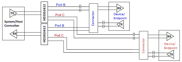 Figure 11. AC Coupling Capacitors Between Switch Tx and Endpoint Tx
In Figure 12, the coupling capacitors are placed on the host transmit pair and endpoint transmit pair. In this situation, the switch on the top is biased by the endpoint and the lower switch is biased by the host controller.
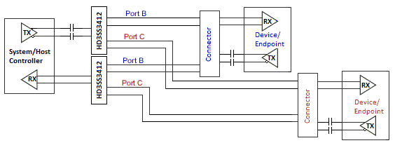 Figure 12. AC Coupling Capacitors on Host Tx and Endpoint Tx
If the common-mode voltage in the system is higher than 2 V, the coupling capacitors are placed on both sides of the switch (shown in Figure 13). A biasing voltage of less than 2 V is required in this case.
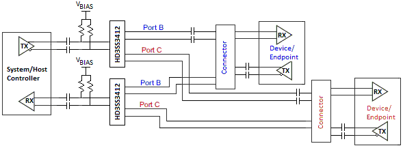 Figure 13. AC Coupling Capacitors on Both Sides of Switch
10.2 Typical Application
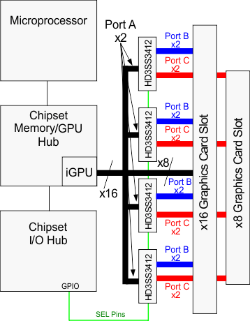 Figure 14. Typical Application Block Diagram
10.2.1 Design Requirements
Table 3 lists the design parameters of this example.
Table 3. Design Parameters
| DESIGN PARAMETERS | EXAMPLE VALUE | |||
|---|---|---|---|---|
| Input voltage range | 3.3 V | |||
| Decoupling capacitors | 0.1 µF | |||
| AC capacitors | 75 nF – 200 nF (100 nF shown) USBAA TX p and n lines require AC capacitors. Alternate mode signals may or may not require AC capacitors | |||
10.2.2 Detailed Design Procedure
- Connect VDD and GND pins to the power and ground planes of the printed circuit board, with 0.1-uF bypass capacitor
- Use +3.3-V TTL/CMOS logic level at SEL
- Use controlled-impedance transmission media for all the differential signals
- Ensure the received complimentary signals are with a differential amplitude of <1800 mVpp and a common-mode voltage of <2 V
10.2.3 Application Curves
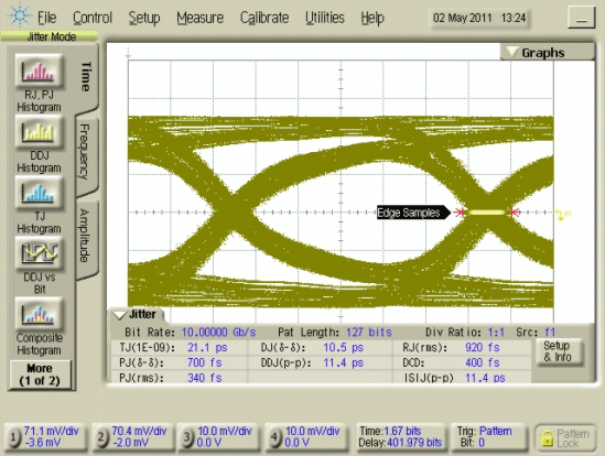 Figure 15. 10-gbps Source Eye Diagram at a: VID = 800 Mvpp; 27–1 Prbs; VCM= 0 V
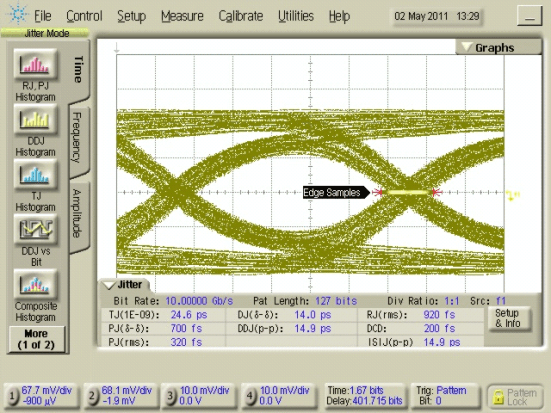 Figure 16. 10-gbps Output Eye Diagram at a: VID = 800 Mvpp; 27–1 Prbs; VCM= 0v; VDD= 3.3 V; Sel= 0 V