SBOS059A November 1996 – February 2024 INA132
PRODUCTION DATA
- 1
- 1Features
- 2Applications
- 3Description
- 4Pin Configuration and Functions
- 5Specifications
- 6Application and Implementation
- 7Device and Documentation Support
- 8Revision History
- 9Mechanical, Packaging, and Orderable Information
Package Options
Refer to the PDF data sheet for device specific package drawings
Mechanical Data (Package|Pins)
- D|8
Thermal pad, mechanical data (Package|Pins)
Orderable Information
4 Pin Configuration and Functions
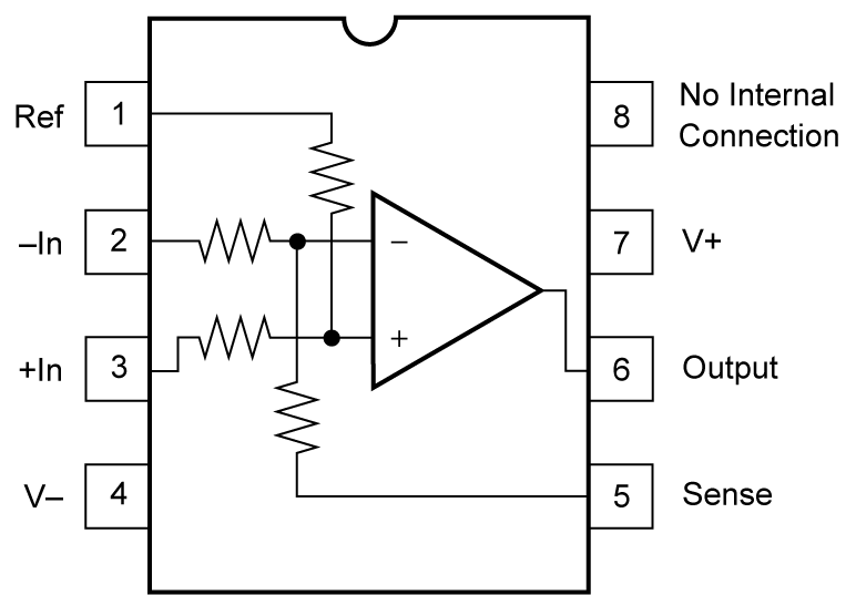
 Figure 4-1 D Package, 8-Pin SOIC (Top
View)
Figure 4-1 D Package, 8-Pin SOIC (Top
View)Table 4-1 Pin Functions
| PIN | TYPE | DESCRIPTION | |
|---|---|---|---|
| NAME | NO. | ||
| –In | 2 | Input | Negative (inverting) input |
| +In | 3 | Input | Positive (noninverting) input |
| No Internal Connection | 8 | — | No internal connection. Leave unconnected. |
| Output | 6 | Output | Output |
| Ref | 1 | — | Reference input. Drive this pin with a low impedance source. Interchanging pin 1 and 3 degrade CMR. |
| Sense | 5 | — | Sense input. Drive this pin with a low impedance source. Interchanging pin 2 and 5 degrade CMR. |
| V– | 4 | Input | Negative supply |
| V+ | 7 | Input | Positive supply |