SGLS174J September   2003  – August 2018 INA138-Q1 , INA168-Q1

PRODUCTION DATA.  

  1. Features
  2. Applications
  3. Description
    1.     Device Images
      1.      Typical Application Circuit
  4. Revision History
  5. Pin Configuration and Functions
    1.     Pin Functions
  6. Specifications
    1. 6.1 Absolute Maximum Ratings
    2. 6.2 ESD Ratings
    3. 6.3 Recommended Operating Conditions
    4. 6.4 Thermal Information
    5. 6.5 Electrical Characteristics
    6. 6.6 Typical Characteristics
  7. Detailed Description
    1. 7.1 Overview
    2. 7.2 Functional Block Diagram
    3. 7.3 Feature Description
      1. 7.3.1 Output Voltage Range
      2. 7.3.2 Bandwidth
    4. 7.4 Device Functional Modes
  8. Application and Implementation
    1. 8.1 Application Information
      1. 8.1.1 Operation
    2. 8.2 Typical Applications
      1. 8.2.1 Buffering Output to Drive an ADC
        1. 8.2.1.1 Design Requirements
        2. 8.2.1.2 Detailed Design Procedure
          1. 8.2.1.2.1 Selecting RS and RL
        3. 8.2.1.3 Application Curve
      2. 8.2.2 Output Filter
        1. 8.2.2.1 Design Requirements
        2. 8.2.2.2 Detailed Design Procedure
        3. 8.2.2.3 Application Curve
      3. 8.2.3 Offsetting the Output Voltage
      4. 8.2.4 Bipolar Current Measurement
        1. 8.2.4.1 Application Curve
      5. 8.2.5 Bipolar Current Measurement Using Differential Input of an ADC
      6. 8.2.6 Multiplexed Measurement Using Logic Signal for Power
  9. Power Supply Recommendations
  10. 10Layout
    1. 10.1 Layout Guidelines
    2. 10.2 Layout Example
  11. 11Device and Documentation Support
    1. 11.1 Documentation Support
      1. 11.1.1 Related Documentation
    2. 11.2 Related Links
    3. 11.3 Receiving Notification of Documentation Updates
    4. 11.4 Community Resources
    5. 11.5 Trademarks
    6. 11.6 Electrostatic Discharge Caution
    7. 11.7 Glossary
  12. 12Mechanical, Packaging, and Orderable Information

Package Options

Mechanical Data (Package|Pins)
Thermal pad, mechanical data (Package|Pins)
Orderable Information

Bipolar Current Measurement

Configure the INA1x8-Q1 as illustrated in Figure 15 for applications where bidirectional current measurement is required. Two INA1x8-Q1 devices are required; connect the inputs across the shunt resistor; see Figure 15. A comparator, such as the TLV3201, is used to detect the polarity of the load current. The magnitude of the load current is monitored across the resistor connected between ground and the connection labeled Output. In this example, the 100-kΩ resistor results in a gain of 20 V/V. The 10-kΩ resistors connected in series with the INA1x8-Q1 output current are used to develop a voltage across the comparator inputs. Two diodes are required to prevent current flow into the INA1x8-Q1 output because only one device at a time provides current to the Output connection of the circuit. The circuit functionality is illustrated in Figure 16.
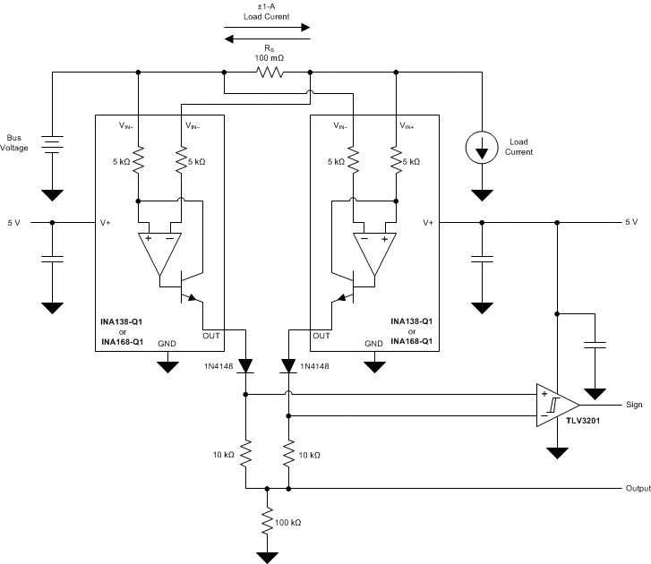
INA138-Q1 INA168-Q1 ai_bi_directional_load_current_sgls174.gifFigure 15. Bipolar Current Measurement