SBOS472B March   2009  – June 2016 INA148-Q1

PRODUCTION DATA.  

  1. Features
  2. Applications
  3. Description
  4. Revision History
  5. Pin Configuration and Functions
  6. Specifications
    1. 6.1 Absolute Maximum Ratings
    2. 6.2 ESD Ratings
    3. 6.3 Recommended Operating Conditions
    4. 6.4 Thermal Information
    5. 6.5 Electrical Characteristics Dual Supply
    6. 6.6 Electrical Characteristics Single Supply
    7. 6.7 Typical Characteristics
  7. Detailed Description
    1. 7.1 Overview
    2. 7.2 Functional Block Diagram
    3. 7.3 Feature Description
      1. 7.3.1 Operating Voltage
      2. 7.3.2 Gain Equation
      3. 7.3.3 Common-Mode Range
      4. 7.3.4 Offset Trim
      5. 7.3.5 Input Impedance
    4. 7.4 Device Functional Modes
  8. Application and Implementation
    1. 8.1 Application Information
    2. 8.2 Typical Applications
      1. 8.2.1 Battery Monitor Circuit
        1. 8.2.1.1 Design Requirements
        2. 8.2.1.2 Detailed Design Procedure
        3. 8.2.1.3 Application Curves
      2. 8.2.2 Quasi-AC-Coupled Differential Amplifier
        1. 8.2.2.1 Design Requirements
        2. 8.2.2.2 Detailed Design Procedure
      3. 8.2.3 Single-Supply Differential Amplifier
        1. 8.2.3.1 Design Requirements
        2. 8.2.3.2 Detailed Design Procedure
      4. 8.2.4 AC-Coupled Difference Amplifier
        1. 8.2.4.1 Design Requirements
        2. 8.2.4.2 Detailed Design Procedure
      5. 8.2.5 50-mV Current-Shunt Amplifier With ±200-V Common-Mode Voltage Range
        1. 8.2.5.1 Design Requirements
        2. 8.2.5.2 Detailed Design Procedure
  9. Power Supply Recommendations
  10. 10Layout
    1. 10.1 Layout Guidelines
    2. 10.2 Layout Example
  11. 11Device and Documentation Support
    1. 11.1 Community Resources
    2. 11.2 Trademarks
    3. 11.3 Electrostatic Discharge Caution
    4. 11.4 Glossary
  12. 12Mechanical, Packaging, and Orderable Information

Package Options

Refer to the PDF data sheet for device specific package drawings

Mechanical Data (Package|Pins)
  • D|8
Thermal pad, mechanical data (Package|Pins)
Orderable Information

10 Layout

10.1 Layout Guidelines

The INA148-Q1 is a precision voltage difference amplifier. To realize the full operational performance of the device, good high-frequency printed-circuit-board (PCB) layout practices are required. Low-loss 0.1-µF bypass capacitors must be connected between each supply pin and ground as close to the device as possible. The bypass capacitor traces must be designed for minimum inductance.

10.2 Layout Example
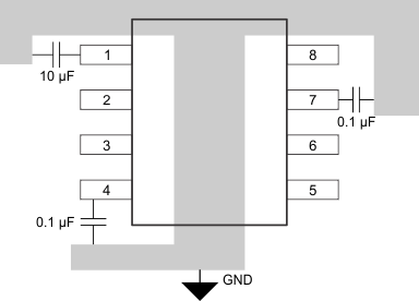
INA148-Q1 INA148_Layout.gif Figure 31. INA148-Q1 Layout Diagram