SBOS741H April   2017  – July 2022 INA180 , INA2180 , INA4180

PRODUCTION DATA  

  1. Features
  2. Applications
  3. Description
  4. Revision History
  5. Device Comparison
  6. Pin Configuration and Functions
  7. Specifications
    1. 7.1 Absolute Maximum Ratings
    2. 7.2 ESD Ratings
    3. 7.3 Recommended Operating Conditions
    4. 7.4 Thermal Information
    5. 7.5 Electrical Characteristics
    6. 7.6 Typical Characteristics
  8. Detailed Description
    1. 8.1 Overview
    2. 8.2 Functional Block Diagrams
    3. 8.3 Feature Description
      1. 8.3.1 High Bandwidth and Slew Rate
      2. 8.3.2 Wide Input Common-Mode Voltage Range
      3. 8.3.3 Precise Low-Side Current Sensing
      4. 8.3.4 Rail-to-Rail Output Swing
    4. 8.4 Device Functional Modes
      1. 8.4.1 Normal Mode
      2. 8.4.2 Input Differential Overload
      3. 8.4.3 Shutdown Mode
  9. Application and Implementation
    1. 9.1 Application Information
      1. 9.1.1 Basic Connections
      2. 9.1.2 RSENSE and Device Gain Selection
      3. 9.1.3 Signal Filtering
    2. 9.2 Typical Application
      1. 9.2.1 Design Requirements
      2. 9.2.2 Detailed Design Procedure
      3. 9.2.3 Application Curve
    3. 9.3 Power Supply Recommendations
      1. 9.3.1 Common-Mode Transients Greater Than 26 V
    4. 9.4 Layout
      1. 9.4.1 Layout Guidelines
      2. 9.4.2 Layout Examples
  10. 10Device and Documentation Support
    1. 10.1 Documentation Support
      1. 10.1.1 Related Documentation
    2. 10.2 Receiving Notification of Documentation Updates
    3. 10.3 Support Resources
    4. 10.4 Trademarks
    5. 10.5 Electrostatic Discharge Caution
    6. 10.6 Glossary
      1.      Mechanical, Packaging, and Orderable Information

Package Options

Mechanical Data (Package|Pins)
Thermal pad, mechanical data (Package|Pins)
Orderable Information

Basic Connections

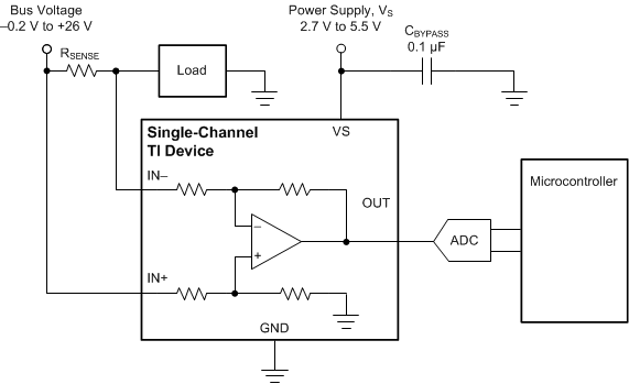
Figure 9-1 shows the basic connections of the INA180. Connect the input pins (IN+ and IN–) as closely as possible to the shunt resistor to minimize any resistance in series with the shunt resistor.
GUID-2E5A9FBF-EABC-4909-8247-FC5C626C9BEB-low.gif
NOTE: For best measurement accuracy, connect analog-to-digital converter (ADC) reference or microcontroller ground as closely as possible to the INAx180 GND pin, and add an RC filter between the output of the INAx180 and the ADC. See Closed-Loop Analysis of Load-Induced Amplifier Stability Issues Using ZOUT for more details.
Figure 9-1 Basic Connections for the INA180

A power-supply bypass capacitor of at least 0.1 µF is required for proper operation. Applications with noisy or high-impedance power supplies may require additional decoupling capacitors to reject power-supply noise. Connect bypass capacitors close to the device pins.