SLYS020C february 2019 – august 2021 INA191 , INA2191
PRODUCTION DATA
- 1
- 1 Features
- 2 Applications
- 3 Description
- 4 Revision History
- 5 Pin Configuration and Functions
- 6 Specifications
- 7 Detailed Description
- 8 Application and Implementation
- 9 Power Supply Recommendations
- 10Layout
- 11Device and Documentation Support
- 12Mechanical, Packaging, and Orderable Information
Package Options
Refer to the PDF data sheet for device specific package drawings
Mechanical Data (Package|Pins)
- YFD|6
Thermal pad, mechanical data (Package|Pins)
Orderable Information
3 Description
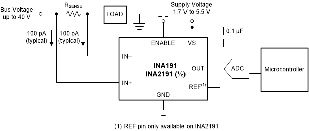
The INAx191 is a low-power, voltage-output, current-shunt monitor (also called a current-sense amplifier) that is commonly used for overcurrent protection, precision-current measurement for system optimization, or in closed-loop feedback circuits. This device can sense drops across shunts at common-mode voltages from –0.2 V to +40 V, independent of the supply voltage. The low input bias current of the INAx191 permits the use of larger current-sense resistors, and thus provides accurate current measurements in the µA range. Five fixed gains are available: 25 V/V, 50 V/V, 100 V/V, 200 V/V, or 500 V/V. The low offset voltage of the zero-drift architecture extends the dynamic range of the current measurement, and allows for smaller sense resistors with lower power loss while still providing accurate current measurements.
The INA191 operates from a single 1.7-V to 5.5-V power supply, drawing a maximum of 65 µA of supply current when enabled and only 100 nA when disabled. The device is specified over the operating temperature range of –40 °C to +125 °C, and offered in a DSBGA-6 (INA191) and DSBGA-12 (INA2191) packages.
| PART NUMBER | PACKAGE | BODY SIZE (NOM) |
|---|---|---|
| INA191 | DSBGA (6) | 1.17 mm × 0.765 mm |
| INA2191 | DSBGA (12) | 1.17 mm × 1.53 mm |
 Simplified Schematic