SBOS781E March 2016 – May 2021 INA199-Q1
PRODUCTION DATA
- 1 Features
- 2 Applications
- 3 Description
- 4 Revision History
- 5 Device Comparison
- 6 Pin Configuration and Functions
- 7 Specifications
- 8 Detailed Description
- 9 Application and Implementation
- 10Power Supply Recommendations
- 11Layout
- 12Device and Documentation Support
- 13Mechanical, Packaging, and Orderable Information
Package Options
Mechanical Data (Package|Pins)
- DCK|6
Thermal pad, mechanical data (Package|Pins)
- DCK|6
Orderable Information
9.1.5 Using the INA199-Q1 With Common-Mode Transients Above 26 V
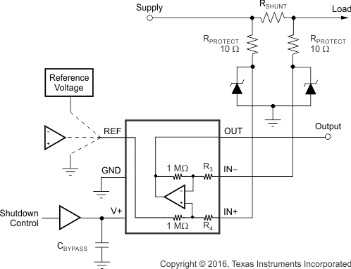
With a small amount of additional circuitry, the INA199-Q1 series can be used in circuits subject to transients higher than 26 V, such as automotive applications. Use only zener diodes or zener-type transient absorbers (sometimes referred to as transzorbs); any other type of transient absorber has an unacceptable time delay. Start by adding a pair of resistors (as shown in Figure 9-5) as a working impedance for the zener. Keeping these resistors as small as possible is preferable, most often approximately 10 Ω. Larger values can be used with an affect on gain as discussed in the Section 9.1.2 section. Many applications are satisfied with a 10-Ω resistor along with conventional zener diodes of the lowest power rating that can be found because this circuit limits only short-term transients. This combination uses the least amount of board space. These diodes can be found in packages as small as SOT-523 or SOD-523. See the TIDA-00302 Transient Robustness for Current Shunt Monitor TI design (TIDU473) for more information on transient robustness and current-shunt monitor input protection.
 Figure 9-5 INA199-Q1 Transient Protection Using Dual Zener Diodes
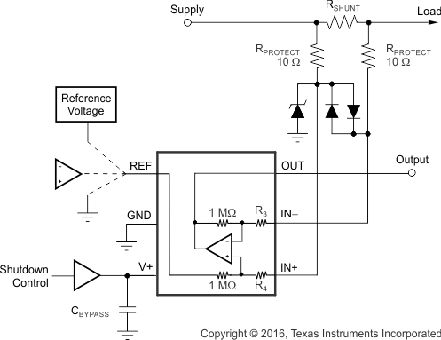
In the event that low-power zeners do not have sufficient transient absorption capability and a higher power transzorb must be used, the most package-efficient solution then involves using a single transzorb and back-to-back diodes between the device inputs. The most space-efficient solutions are dual series-connected diodes in a single SOT-523 or SOD-523 package. This method is illustrated in Figure 9-6. In either of these examples, the total board area required by the INA199-Q1 with all protective components is less than that of an 8-pin SOIC package, and only slightly greater than that of an 8-pin VSSOP package.
 Figure 9-6 INA199-Q1 Transient Protection Using a Single Transzorb and Input Clamps