SLOS785B June   2012  – March 2016 INA220-Q1

PRODUCTION DATA.  

  1. Features
  2. Applications
  3. Description
  4. Revision History
  5. Related Products
  6. Pin Configuration and Functions
  7. Specifications
    1. 7.1 Absolute Maximum Ratings
    2. 7.2 ESD Ratings
    3. 7.3 Recommended Operating Conditions
    4. 7.4 Thermal Information
    5. 7.5 Electrical Characteristics
    6. 7.6 Typical Characteristics
  8. Detailed Description
    1. 8.1 Overview
    2. 8.2 Functional Block Diagram
    3. 8.3 Feature Description
      1. 8.3.1 Basic ADC Functions
        1. 8.3.1.1 Power Measurement
        2. 8.3.1.2 PGA Function
    4. 8.4 Device Functional Modes
      1. 8.4.1 Filtering and Input Considerations
    5. 8.5 Programming
      1. 8.5.1 Programming the INA220-Q1 Calibration Register
      2. 8.5.2 Programming the INA220-Q1 Power Measurement Engine
        1. 8.5.2.1 Calibration Register and Scaling
      3. 8.5.3 Simple Current Shunt Monitor Usage (No Programming Necessary)
      4. 8.5.4 Bus Overview
        1. 8.5.4.1 Serial Bus Address
        2. 8.5.4.2 Serial Interface
      5. 8.5.5 Writing to and Reading from the INA220-Q1
        1. 8.5.5.1 High-Speed Mode
        2. 8.5.5.2 Power-Up Conditions
    6. 8.6 Register Maps
      1. 8.6.1 Register Information
      2. 8.6.2 Register Details
        1. 8.6.2.1 Configuration Register (address = 00h) [reset = 399Fh]
      3. 8.6.3 Data Output Registers
        1. 8.6.3.1 Shunt Voltage Register (address = 01h)
        2. 8.6.3.2 Bus Voltage Register (address = 02h)
        3. 8.6.3.3 Power Register (address = 03h) [reset = 00h]
        4. 8.6.3.4 Current Register (address = 04h) [reset =00h]
      4. 8.6.4 Calibration Register
        1. 8.6.4.1 Calibration Register (address = 05h) [reset = 00h]
  9. Application and Implementation
    1. 9.1 Application Information
    2. 9.2 Typical Application
      1. 9.2.1 Design Requirements
      2. 9.2.2 Detailed Design Procedure
        1. 9.2.2.1 Register Results for the Example Circuit
    3. 9.3 System Examples
  10. 10Power Supply Recommendations
  11. 11Layout
    1. 11.1 Layout Guidelines
    2. 11.2 Layout Example
  12. 12Device and Documentation Support
    1. 12.1 Related Documentation
    2. 12.2 Community Resources
    3. 12.3 Trademarks
    4. 12.4 Electrostatic Discharge Caution
    5. 12.5 Glossary
  13. 13Mechanical, Packaging, and Orderable Information

Package Options

Mechanical Data (Package|Pins)
Thermal pad, mechanical data (Package|Pins)
Orderable Information

6 Pin Configuration and Functions

DGS Package
10-Pin VSSOP
Top View
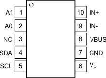
INA220-Q1 po_msop_bos459.gif

Pin Functions

PIN I/O DESCRIPTION
NO. NAME
1 A1 Digital Input Address pin. Connect to GND, SCL, SDA, or VS. Table 1 shows pin settings and corresponding addresses.
2 A0 Digital Input Address pin. Connect to GND, SCL, SDA, or VS. Table 1 shows pin settings and corresponding addresses.
3 NC No internal connection
4 SDA Digital I/O Serial bus data line
5 SCL Digital Input Serial bus clock line
6 VS Analog Power supply, 3 V to 5.5 V
7 GND Analog Ground
8 VBUS Analog Input Bus voltage input
9 IN– Analog Input Negative differential shunt voltage. Connect to negative side of shunt resistor. Bus voltage is measured from this pin to ground.
10 IN+ Analog Input Positive differential shunt voltage. Connect to positive side of shunt resistor.