SBOS728A February 2015 – March 2021 INA225-Q1
PRODUCTION DATA
- 1 Features
- 2 Applications
- 3 Description
- 4 Revision History
- 5 Pin Configuration and Functions
- 6 Specifications
- 7 Detailed Description
- 8 Applications and Implementation
- 9 Power Supply Recommendations
- 10Layout
- 11Device and Documentation Support
- 12Mechanical, Packaging, and Orderable Information
Package Options
Mechanical Data (Package|Pins)
- DGK|8
Thermal pad, mechanical data (Package|Pins)
Orderable Information
7.4.3 Using the Device with Common-Mode Transients Above 36 V
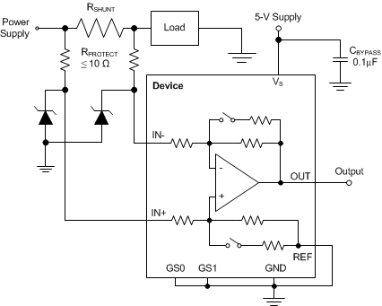
With a small amount of additional circuitry, the
device can be used in circuits subject to transients higher than
36 V (such as automotive
applications). Use only zener diodes or zener-type transient
absorbers (sometimes referred to as transzorbs); any other
type of transient absorber has an unacceptable time delay. Start by
adding a pair of resistors, as shown in Figure 7-3, as a working impedance for the zener. Keeping these resistors as
small as possible is preferable, most often around 10 Ω. This value
limits the impact on accuracy with the addition of these external
components, as described in the Section 7.4.1 section. Larger values can be used if necessary with
the result having an impact on gain error. Because this circuit
limits only short-term transients, many applications are satisfied
with a 10-Ω resistor along with conventional zener diodes of the
lowest power rating available. This combination uses the least
amount of board space. These diodes can be found in packages as
small as SOT-523 or SOD-523.
 Figure 7-3 Device Transient Protection