SBOS808E August   2016  – December 2021 INA240-Q1

PRODUCTION DATA  

  1. Features
  2. Applications
  3. Description
  4. Revision History
  5. Device Comparison
  6. Pin Configuration and Functions
  7. Specifications
    1. 7.1 Absolute Maximum Ratings
    2. 7.2 ESD Ratings
    3. 7.3 Recommended Operating Conditions
    4. 7.4 Thermal Information
    5. 7.5 Electrical Characteristics
    6. 7.6 Typical Characteristics
  8. Detailed Description
    1. 8.1 Overview
    2. 8.2 Functional Block Diagram
    3. 8.3 Feature Description
      1. 8.3.1 Amplifier Input Signal
        1. 8.3.1.1 Enhanced PWM Rejection Operation
        2. 8.3.1.2 Input Signal Bandwidth
      2. 8.3.2 Selecting the Sense Resistor (RSENSE)
    4. 8.4 Device Functional Modes
      1. 8.4.1 Adjusting the Output Midpoint With the Reference Pins
      2. 8.4.2 Reference Pin Connections for Unidirectional Current Measurements
        1. 8.4.2.1 Ground Referenced Output
        2. 8.4.2.2 VS Referenced Output
      3. 8.4.3 Reference Pin Connections for Bidirectional Current Measurements
        1. 8.4.3.1 Output Set to External Reference Voltage
        2. 8.4.3.2 Output Set to Midsupply Voltage
        3. 8.4.3.3 Output Set to Mid-External Reference
        4. 8.4.3.4 Output Set Using Resistor Divider
      4. 8.4.4 Calculating Total Error
        1. 8.4.4.1 Error Sources
        2. 8.4.4.2 Reference Voltage Rejection Ratio Error
          1. 8.4.4.2.1 Total Error Example 1
          2. 8.4.4.2.2 Total Error Example 2
  9. Application and Implementation
    1. 9.1 Application Information
      1. 9.1.1 Input Filtering
    2. 9.2 Typical Applications
      1. 9.2.1 Inline Motor Current-Sense Application
        1. 9.2.1.1 Design Requirements
        2. 9.2.1.2 Detailed Design Procedure
        3. 9.2.1.3 Application Curve
      2. 9.2.2 Solenoid Drive Current-Sense Application
        1. 9.2.2.1 Design Requirements
        2. 9.2.2.2 Detailed Design Procedure
        3. 9.2.2.3 Application Curve
    3. 9.3 What to Do and What Not to Do
      1. 9.3.1 High-Precision Applications
      2. 9.3.2 Kelvin Connection from the Current-Sense Resistor
  10. 10Power Supply Recommendations
    1. 10.1 Power Supply Decoupling
  11. 11Layout
    1. 11.1 Layout Guidelines
      1. 11.1.1 Connection to the Current-Sense Resistor
    2. 11.2 Layout Example
  12. 12Device and Documentation Support
    1. 12.1 Documentation Support
      1. 12.1.1 Related Documentation
    2. 12.2 Receiving Notification of Documentation Updates
    3. 12.3 Support Resources
    4. 12.4 Trademarks
    5. 12.5 Electrostatic Discharge Caution
    6. 12.6 Glossary
  13. 13Mechanical, Packaging, and Orderable Information

Package Options

Mechanical Data (Package|Pins)
Thermal pad, mechanical data (Package|Pins)
Orderable Information

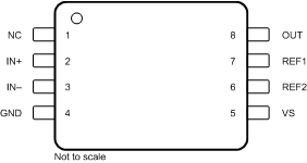
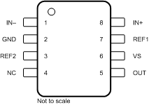
Pin Configuration and Functions

GUID-74758157-BCBB-4150-9BF7-CB822CF9E918-low.gif
NC- no internal connection
For INA240-Q1, Grade 1 only
Figure 6-1 INA240-Q1 PW Package8-Pin TSSOPTop View
GUID-6982B0C2-EF83-4812-953E-4325678107DF-low.gif
NC- no internal connection
For INA240-Q1, Grade 0 and Grade 1
Figure 6-2 INA240-Q1 D Package8-Pin SOICTop View
Table 6-1 Pin Functions
PIN I/O DESCRIPTION
NAME PW (TSSOP) D
(SOIC)
GND 4 2 Analog Ground
IN– 3 1 Analog input Connect to load side of shunt resistor
IN+ 2 8 Analog input Connect to supply side of shunt resistor
NC 1 4 Reserved. Connect to ground or leave floating
OUT 8 5 Analog output Output voltage
REF1 7 7 Analog input Reference 1 voltage. Connect to 0 V to VS; see the Section 8.4.1 section for connection options
REF2 6 3 Analog input Reference 2 voltage. Connect to 0 V to VS; see the Section 8.4.1 section for connection options
VS 5 6 Power supply, 2.7 V to 5.5 V