SBOS511C April 2015 – September 2023
PRODUCTION DATA
- 1
- 1 Features
- 2 Applications
- 3 Description
- 4 Revision History
- 5 Pin Configuration and Functions
- 6 Specifications
- 7 Detailed Description
- 8 Applications and Implementation
- 9 Device and Documentation Support
- 10Mechanical, Packaging, and Orderable Information
Package Options
Mechanical Data (Package|Pins)
- PW|16
Thermal pad, mechanical data (Package|Pins)
Orderable Information
3 Description
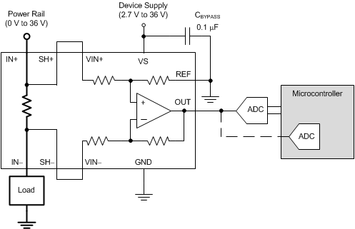
The INA250 is a voltage-output, current-sensing amplifier family that integrates an internal shunt resistor to enable high-accuracy current measurements at common-mode voltages that can vary from 0 V to 36 V, independent of the supply voltage. The device is a bidirectional, low- or high-side current-shunt monitor that allows an external reference to be used to measure current flowing in both directions through the internal current-sensing resistor sensor. The integration of the precision current-sensing resistor provides calibration equivalent measurement accuracy with ultra-low temperature drift performance and ensures an optimized Kelvin layout for the sensing resistor is always obtained.
The INA250 family is available in four output voltage scales: 200 mV/A, 500 mV/A, 800 mV/A, and 2 V/A. This device is fully tested and specified for continuous currents up to 10 amps at the maximum temperature of 125°C. The INA250 operates from a single 2.7-V to 36-V supply and draws a maximum of 300 µA of supply current. All INA250 gain versions are specified over the extended operating temperature range (–40°C to 125°C), and are available in a TSSOP-16 package.
| PART NUMBER | PACKAGE(1) | PACKAGE SIZE(2) |
|---|---|---|
| INA250A1 | PW (TSSOP, 16) | 5.00 mm × 6.40 mm |
| INA250A2 | ||
| INA250A3 | ||
| INA250A4 |
 Simplified Schematic