SBOS381E February   2007  – January 2018 INA270 , INA271

PRODUCTION DATA.  

  1. Features
  2. Applications
  3. Description
    1.     Device Images
      1.      Simplified Schematic
  4. Revision History
  5. Device Comparison Table
  6. Pin Configuration and Functions
    1.     Pin Functions
  7. Specifications
    1. 7.1 Absolute Maximum Ratings
    2. 7.2 ESD Ratings
    3. 7.3 Recommended Operating Conditions
    4. 7.4 Thermal Information
    5. 7.5 Electrical Characteristics
    6. 7.6 Typical Characteristics
  8. Detailed Description
    1. 8.1 Overview
    2. 8.2 Functional Block Diagram
    3. 8.3 Feature Description
      1. 8.3.1 Basic Connection
      2. 8.3.2 Selecting RS
      3. 8.3.3 Transient Protection
    4. 8.4 Device Functional Modes
      1. 8.4.1 First- or Second-Order Filtering
      2. 8.4.2 Accuracy Variations as a Result of VSENSE and Common-Mode Voltage
        1. 8.4.2.1 Normal Case 1: VSENSE ≥ 20 mV, VCM ≥ VS
        2. 8.4.2.2 Normal Case 2: VSENSE ≥ 20 mV, VCM < VS
        3. 8.4.2.3 Low VSENSE Case 1: VSENSE < 20 mV, –16 V ≤ VCM < 0; and Low VSENSE Case 3: VSENSE < 20 mV, VS < VCM ≤ 80 V
        4. 8.4.2.4 Low VSENSE Case 2: VSENSE < 20 mV, 0 V ≤ VCM ≤ VS
  9. Application and Implementation
    1. 9.1 Application Information
    2. 9.2 Typical Application
      1. 9.2.1 Design Requirements
      2. 9.2.2 Detailed Design Procedure
      3. 9.2.3 Application Curves
  10. 10Power Supply Recommendations
    1. 10.1 Shutdown
  11. 11Layout
    1. 11.1 Layout Guidelines
      1. 11.1.1 RFI and EMI
    2. 11.2 Layout Example
  12. 12Device and Documentation Support
    1. 12.1 Documentation Support
      1. 12.1.1 Related Documentation
    2. 12.2 Related Links
    3. 12.3 Community Resources
    4. 12.4 Trademarks
    5. 12.5 Electrostatic Discharge Caution
    6. 12.6 Glossary
  13. 13Mechanical, Packaging, and Orderable Information

Package Options

Mechanical Data (Package|Pins)
Thermal pad, mechanical data (Package|Pins)
Orderable Information

Pin Configuration and Functions

D Package
SOIC-8
Top View
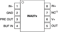
INA270 INA271 po_bos381.gif

NOINDENT:

NOTE (1): NC denotes no internal connection.

Pin Functions

PINI/ODESCRIPTION
NAMENO.
BUF IN 4 Analog input Connect to output of filter from PRE OUT
GND 2 Analog Ground
IN– 1 Analog input Connect to load side of shunt resistor
IN+ 8 Analog input Connect to supply side of shunt resistor
NC 7 Connect to ground
OUT 5 Analog output Output voltage
PRE OUT 3 Analog output Connect to input of filter to BUF IN
V+ 6 Analog input Power supply, +2.7 V to +18 V