SBOS485C November 2009 – May 2015 INA282 , INA283 , INA284 , INA285 , INA286
PRODUCTION DATA.
- 1 Features
- 2 Applications
- 3 Description
- 4 Revision History
- 5 Pin Configuration and Functions
- 6 Specifications
- 7 Detailed Description
- 8 Applications and Implementation
- 9 Power Supply Recommendations
- 10Layout
- 11Device and Documentation Support
- 12Mechanical, Packaging, and Orderable Information
Package Options
Mechanical Data (Package|Pins)
Thermal pad, mechanical data (Package|Pins)
- DGK|8
Orderable Information
6 Specifications
6.1 Absolute Maximum Ratings
Over operating free-air temperature range (unless otherwise noted)(1)| MIN | MAX | UNIT | ||
|---|---|---|---|---|
| Supply voltage, V+ | 18 | V | ||
| Analog inputs, V+IN, V–IN(2) | Differential (V+IN) – (V–IN)(3) | –5 | +5 | V |
| Common-mode | –14 | +80 | V | |
| REF1, REF2, OUT | GND – 0.3 | (V+) + 0.3 | V | |
| Input current into any pin | 5 | mA | ||
| Junction temperature | 150 | °C | ||
| Storage temperature range, Tstg | –65 | +150 | °C | |
(1) Stresses beyond those listed under Absolute Maximum Ratings may cause permanent damage to the device. These are stress ratings only, which do not imply functional operation of the device at these or any other conditions beyond those indicated under Recommended Operating Conditions. Exposure to absolute-maximum-rated conditions for extended periods may affect device reliability.
(2) V+IN and V–IN are the voltages at the +IN and –IN pins, respectively.
(3) Input voltages must not exceed common-mode rating.
6.2 ESD Ratings
| VALUE | UNIT | |||
|---|---|---|---|---|
| V(ESD) | Electrostatic discharge | Human-body model (HBM), per ANSI/ESDA/JEDEC JS-001(1) | ±2000 | V |
| Charged-device model (CDM), per JEDEC specification JESD22-C101(2) | ±1000 | |||
(1) JEDEC document JEP155 states that 500-V HBM allows safe manufacturing with a standard ESD control process.
(2) JEDEC document JEP157 states that 250-V CDM allows safe manufacturing with a standard ESD control process.
6.3 Recommended Operating Conditions
over operating free-air temperature range (unless otherwise noted)| MIN | NOM | MAX | UNIT | ||
|---|---|---|---|---|---|
| VCM | Common-mode input voltage | 12 | V | ||
| V+ | Operating supply voltage | 5 | V | ||
| TA | Operating free-air temperature | –40 | +125 | °C | |
6.4 Thermal Information
| THERMAL METRIC(1) | INA28x | UNIT | ||
|---|---|---|---|---|
| D (SOIC) | DGK (VSSOP) | |||
| 8 PINS | 8 PINS | |||
| RθJA | Junction-to-ambient thermal resistance | 134.9 | 164.1 | °C/W |
| RθJC(top) | Junction-to-case (top) thermal resistance | 72.9 | 56.4 | °C/W |
| RθJB | Junction-to-board thermal resistance | 61.3 | 85.0 | °C/W |
| ψJT | Junction-to-top characterization parameter | 18.9 | 6.5 | °C/W |
| ψJB | Junction-to-board characterization parameter | 54.3 | 83.3 | °C/W |
| RθJC(bot) | Junction-to-case (bottom) thermal resistance | n/a | n/a | °C/W |
(1) For more information about traditional and new thermal metrics, see the Semiconductor and IC Package Thermal Metrics application report, SPRA953.
6.5 Electrical Characteristics
At TA = 25°C, V+ = 5 V, V+IN = 12 V, VREF1 = VREF2 = 2.048 V referenced to GND, and VSENSE = V+IN – V–IN (unless otherwise noted)| PARAMETER | TEST CONDITIONS | MIN | TYP | MAX | UNIT | ||
|---|---|---|---|---|---|---|---|
| INPUT | |||||||
| VOS | Offset voltage, RTI(1) | VSENSE = 0 mV | ±20 | ±70 | µV | ||
| dVOS/dT | vs temperature | VSENSE = 0 mV, TA = –40°C to +125°C |
±0.3 | ±1.5 | µV/°C | ||
| PSRR | vs power supply | V+ = +2.7 V to +18 V, VSENSE = 0 mV |
3 | μV/V | |||
| VCM | Common-mode input range | TA = –40°C to +125°C | –14 | +80 | V | ||
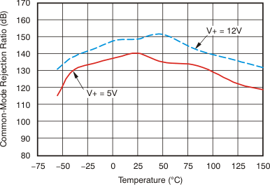
| CMRR | Common-mode rejection ratio | V+IN = –14 V to +80 V, VSENSE = 0 mV, TA = –40°C to +125°C |
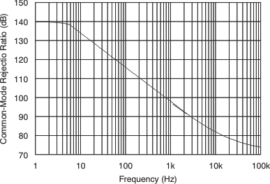
120 | 140 | dB | ||
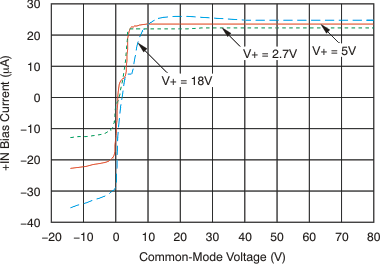
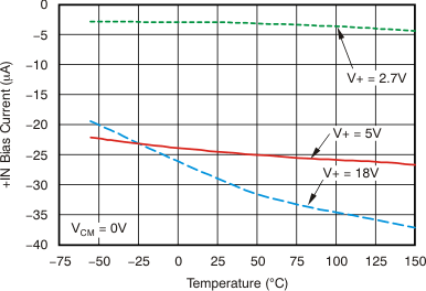
| IB | Input bias current per pin(2) | VSENSE = 0 mV | 25 | µA | |||
| IOS | Input offset current | VSENSE = 0 mV | 1 | µA | |||
| Differential input impedance | 6 | kΩ | |||||
| REFERENCE INPUTS | |||||||
| Reference input gain | 1 | V/V | |||||
| Reference input voltage range(3) | 0 | VGND + 9 | V | ||||
| Divider accuracy(4) | ±0.2% | ±0.5% | |||||
| RVRR | Reference voltage rejection ratio (VREF1 = VREF2 = 40 mV to 9 V, V+ = 18 V) |
INA282 | ±25 | ±75 | µV/V | ||
| TA = –40°C to +125°C | 0.055 | µV/V/°C | |||||
| INA283 | ±13 | ±30 | µV/V | ||||
| TA = –40°C to +125°C | 0.040 | µV/V/°C | |||||
| INA284 | ±6 | ±25 | µV/V | ||||
| TA = –40°C to +125°C | 0.015 | µV/V/°C | |||||
| INA285 | ±4 | ±10 | µV/V | ||||
| TA = –40°C to +125°C | 0.010 | µV/V/°C | |||||
| INA286 | ±17 | ±45 | µV/V | ||||
| TA = –40°C to +125°C | 0.040 | µV/V/°C | |||||
| GAIN(5) (GND + 0.5 V ≤ VOUT ≤ (V+) – 0.5 V; VREF1 = VREF2 = (V+) / 2 for all devices) | |||||||
| G | Gain | INA282, V+ = 5 V | 50 | V/V | |||
| INA283, V+ = 5 V | 200 | V/V | |||||
| INA284, V+ = 12 V | 500 | V/V | |||||
| INA285, V+ = 12 V | 1000 | V/V | |||||
| INA286, V+ = 5 V | 100 | V/V | |||||
| Gain error | INA282, INA283, INA286 | ±0.4% | ±1.4% | ||||
| INA284, INA285 | ±0.4% | ±1.6% | |||||
| TA = –40°C to +125°C | 0.0008 | 0.005 | %/°C | ||||
| OUTPUT | |||||||
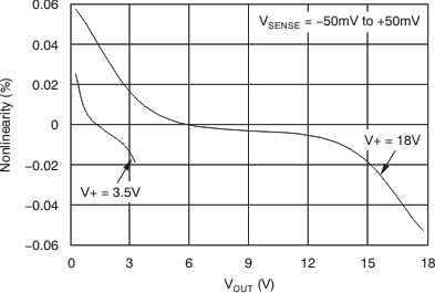
| Nonlinearity error | ±0.01% | ||||||
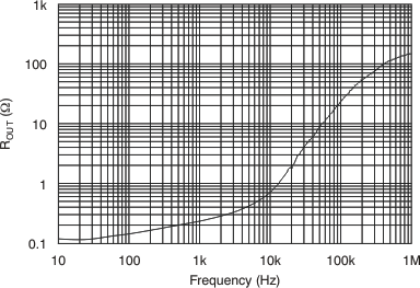
| Output impedance | 1.5 | Ω | |||||
| Maximum capacitive load | No sustained oscillation | 1 | nF | ||||
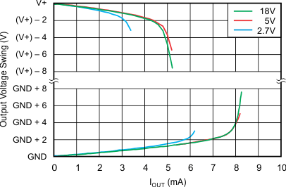
| VOLTAGE OUTPUT(6) | |||||||
| Swing to V+ power-supply rail | V+ = 5 V, RLOAD = 10 kΩ to GND, TA = –40°C to +125°C |
(V+) – 0.17 | (V+) – 0.4 | V | |||
| Swing to GND | RLOAD = 10 kΩ to GND, TA = –40°C to +125°C |
GND + 0.015 | GND + 0.04 | V | |||
| FREQUENCY RESPONSE | |||||||
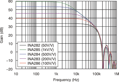
| BW | Effective bandwidth(7) | INA282 | 10 | kHz | |||
| INA283 | 10 | kHz | |||||
| INA284 | 4 | kHz | |||||
| INA285 | 2 | kHz | |||||
| INA286 | 10 | kHz | |||||
| NOISE, RTI(1) | |||||||
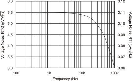
| Voltage noise density | 1 kHz | 110 | nV/√Hz | ||||
| POWER SUPPLY | |||||||
| VS | Specified voltage range | TA = –40°C to +125°C | 2.7 | 18 | V | ||
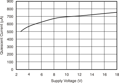
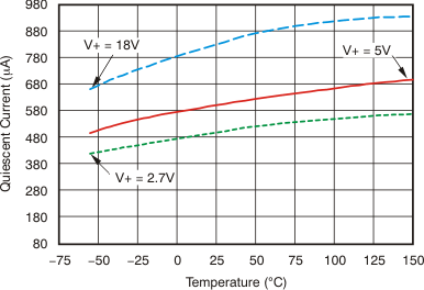
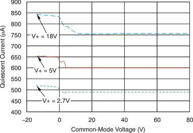
| IQ | Quiescent current | 600 | 900 | µA | |||
(1) RTI = referred-to-input.
(2) See typical characteristic graph Figure 7.
(3) The average of the voltage on pins REF1 and REF2 must be between VGND and the lesser of (VGND + 9 V) and V+.
(4) Reference divider accuracy specifies the match between the reference divider resistors using the configuration in Figure 36.
(5) See typical characteristic graph Figure 12.
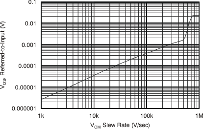
(7) See typical characteristic graph Figure 1 and the Effective Bandwidth section.
6.6 Typical Characteristics
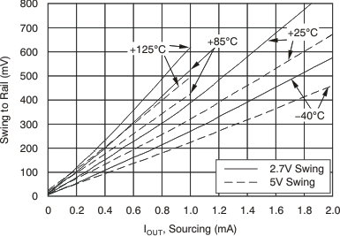
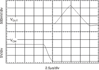
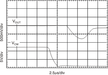
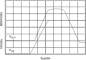
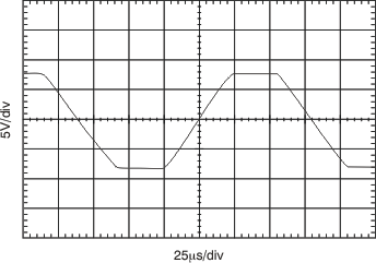
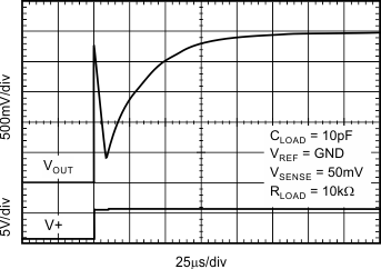
At TA = 25°C, V+ = 5 V, V+IN = 12 V, VREF1 = VREF2 = 2.048 V referenced to GND, and VSENSE = V+IN – V–IN (unless otherwise noted)