SLLSEY7F June   2017  – April 2020 ISO1211 , ISO1212

PRODUCTION DATA.  

  1. Features
  2. Applications
  3. Description
    1.     Device Images
      1.          Application Diagram
      2.      ISO121x Devices Reduce Board Temperatures vs Traditional Solutions
  4. Revision History
  5. Pin Configuration and Functions
    1.     Pin Functions
    2.     Pin Functions
  6. Specifications
    1. 6.1  Absolute Maximum Ratings
    2. 6.2  ESD Ratings
    3. 6.3  Recommended Operating Conditions
    4. 6.4  Thermal Information
    5. 6.5  Power Ratings
    6. 6.6  Insulation Specifications
    7. 6.7  Safety-Related Certifications
    8. 6.8  Safety Limiting Values
    9. 6.9  Electrical Characteristics—DC Specification
    10. 6.10 Switching Characteristics—AC Specification
    11. 6.11 Insulation Characteristics Curves
    12. 6.12 Typical Characteristics
  7. Parameter Measurement Information
    1. 7.1 Test Circuits
  8. Detailed Description
    1. 8.1 Overview
    2. 8.2 Functional Block Diagram
    3. 8.3 Feature Description
    4. 8.4 Device Functional Modes
  9. Application and Implementation
    1. 9.1 Application Information
    2. 9.2 Typical Application
      1. 9.2.1 Sinking Inputs
        1. 9.2.1.1 Design Requirements
        2. 9.2.1.2 Detailed Design Procedure
          1. 9.2.1.2.1 Setting Current Limit and Voltage Thresholds
          2. 9.2.1.2.2 Thermal Considerations
          3. 9.2.1.2.3 Designing for 48-V Systems
          4. 9.2.1.2.4 Designing for Input Voltages Greater Than 60 V
          5. 9.2.1.2.5 Surge, ESD, and EFT Tests
          6. 9.2.1.2.6 Multiplexing the Interface to the Host Controller
          7. 9.2.1.2.7 Status LEDs
        3. 9.2.1.3 Application Curve
      2. 9.2.2 Sourcing Inputs
      3. 9.2.3 Sourcing and Sinking Inputs (Bidirectional Inputs)
  10. 10Power Supply Recommendations
  11. 11Layout
    1. 11.1 Layout Guidelines
    2. 11.2 Layout Example
  12. 12Device and Documentation Support
    1. 12.1 Device Support
      1. 12.1.1 Development Support
    2. 12.2 Documentation Support
      1. 12.2.1 Related Documentation
    3. 12.3 Related Links
    4. 12.4 Receiving Notification of Documentation Updates
    5. 12.5 Community Resource
    6. 12.6 Trademarks
    7. 12.7 Electrostatic Discharge Caution
    8. 12.8 Glossary
  13. 13Mechanical, Packaging, and Orderable Information

Package Options

Refer to the PDF data sheet for device specific package drawings

Mechanical Data (Package|Pins)
  • D|8
Thermal pad, mechanical data (Package|Pins)
Orderable Information

Pin Configuration and Functions

ISO1211 D Package
8-Pin SOIC
Top View
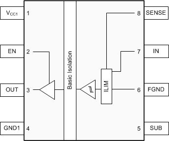
ISO1211 ISO1212 pin_config_sllu258.gif

Pin Functions

PIN I/O DESCRIPTION
NO. NAME
1 VCC1 Power supply, side 1
2 EN I Output enable. The output pin on side 1 is enabled when the EN pin is high or open. The output pin on side 1 is in the high-impedance state when the EN pin is low. In noisy applications, tie the EN pin to VCC1.
3 OUT O Channel output
4 GND1 Ground connection for VCC1
5 SUB Internal connection to input chip substrate. For good thermal performance, it is recommended to connect this pin to a small 2 mm x 2 mm floating plane on the board. Do not connect this floating plane to FGND or any other signal or plane.
6 FGND Field-side ground
7 IN I Field-side current input
8 SENSE I Field-side voltage sense
ISO1212 DBQ Package
16-Pin SSOP
Top View
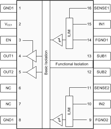
ISO1211 ISO1212 iso1212-isolated-digital-input-receiver-pin-configuration.gif

Pin Functions

PIN I/O Description
NO. NAME
1 GND1 Ground connection for VCC1
2 VCC1 Power supply, side 1
3 EN I Output enable. The output pins on side 1 are enabled when the EN pin is high or open. The output pins on side 1 are in the high-impedance state when the EN pin is low. In noisy applications, tie the EN pin to VCC1.
4 OUT1 O Channel 1 output
5 OUT2 O Channel 2 output
6 NC Not connected
7
8 GND1 Ground connection for VCC1
9 FGND2 Field-side ground, channel 2
10 IN2 I Field-side current input, channel 2
11 SENSE2 I Field-side voltage sense, channel 2
12 SUB2 Internal connection to input chip 2 substrate. For good thermal performance, it is recommended to connect this pin to a small 2 mm x 2 mm floating plane on the board. Do not connect this floating plane to FGND1, FGND2, SUB1 or any other signal or plane.
13 SUB1 Internal connection to input chip 1 substrate. For good thermal performance, it is recommended to connect this pin to a small 2 mm x 2 mm floating plane on the board. Do not connect this floating plane to FGND1, FGND2, SUB2 or any other signal or plane.
14 FGND1 Field-side ground, channel 1
15 IN1 I Field-side current input, channel 1
16 SENSE1 I Field-side voltage sense, channel 1