SLLSFG1B February 2020 – December 2020 ISOW7841A-Q1
PRODUCTION DATA
- 1 Features
- 2 Applications
- 3 Description
- 4 Revision History
- 5 Description Continued
- 6 Pin Configuration and Functions
-
7 Specifications
- 7.1 Absolute Maximum Ratings
- 7.2 ESD Ratings
- 7.3 Recommended Operating Conditions
- 7.4 Thermal Information
- 7.5 Power Ratings
- 7.6 Insulation Specifications
- 7.7 Safety-Related Certifications
- 7.8 Safety Limiting Values
- 7.9 Electrical Characteristics—5-V Input, 5-V Output
- 7.10 Supply Current Characteristics—5-V Input, 5-V Output
- 7.11 Electrical Characteristics—3.3-V Input, 5-V Output
- 7.12 Supply Current Characteristics—3.3-V Input, 5-V Output
- 7.13 Electrical Characteristics—5-V Input, 3.3-V Output
- 7.14 Supply Current Characteristics—5-V Input, 3.3-V Output
- 7.15 Electrical Characteristics—3.3-V Input, 3.3-V Output
- 7.16 Supply Current Characteristics—3.3-V Input, 3.3-V Output
- 7.17 Switching Characteristics—5-V Input, 5-V Output
- 7.18 Switching Characteristics—3.3-V Input, 5-V Output
- 7.19 Switching Characteristics—5-V Input, 3.3-V Output
- 7.20 Switching Characteristics—3.3-V Input, 3.3-V Output
- 7.21 Insulation Characteristics Curves
- 7.22 Typical Characteristics
- 8 Parameter Measurement Information
- 9 Detailed Description
- 10Application and Implementation
- 11Layout
- 12Device and Documentation Support
- 13Mechanical, Packaging, and Orderable Information
Package Options
Mechanical Data (Package|Pins)
- DWE|16
Thermal pad, mechanical data (Package|Pins)
Orderable Information
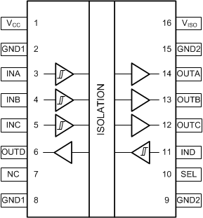
6 Pin Configuration and Functions
 ISOW7841A-Q1 DWE Package.
16-Pin SOIC-WB. Top View.
 Table 6-1 Pin Functions
| PIN | I/O | DESCRIPTION | |||||
|---|---|---|---|---|---|---|---|
| NAME | NO. | ||||||
| ISOW7841A-Q1 | |||||||
| GND1 | 2, 8 | — | Ground connection for VCC | ||||
| GND2 | 9, 15 | — | Ground connection for VISO | ||||
| INA | 3 | I | Input channel A | ||||
| INB | 4 | I | Input channel B | ||||
| INC | 5 | I | Input channel C | ||||
| IND | 11 | I | Input channel D | ||||
| NC | 7 | — | Not connected | ||||
| OUTA | 14 | O | Output channel A | ||||
| OUTB | 13 | O | Output channel B | ||||
| OUTC | 12 | O | Output channel C | ||||
| OUTD | 6 | O | Output channel D | ||||
| SEL | 10 | I | VISO selection pin. VISO = 5 V when SEL shorted to VISO. VISO = 3.3 V, when SEL shorted to GND2 or when left floating. For more information see Section 9.4. | ||||
| VCC | 1 | — | Supply voltage | ||||
| VISO | 16 | — | Isolated supply voltage determined by SEL pin | ||||