SNOSBI3C July 2000 – October 2018 LF198-N , LF298 , LF398-N
PRODUCTION DATA.
- 1 Features
- 2 Applications
- 3 Description
- 4 Revision History
- 5 Pin Configuration and Functions
-
6 Specifications
- 6.1 Absolute Maximum Ratings
- 6.2 Recommended Operating Conditions
- 6.3 Thermal Information
- 6.4 Electrical Characteristics, LF198-N and LF298
- 6.5 Electrical Characteristics, LF198A-N
- 6.6 Electrical Characteristics, LF398-N
- 6.7 Electrical Characteristics, LF398A-N (OBSOLETE)
- 6.8 Typical Characteristics
- 7 Parameter Measurement Information
- 8 Detailed Description
-
9 Application and Implementation
- 9.1 Application Information
- 9.2
Typical Applications
- 9.2.1 X1000 Sample and Hold
- 9.2.2 Sample and Difference Circuit
- 9.2.3 Ramp Generator With Variable Reset Level
- 9.2.4 Integrator With Programmable Reset Level
- 9.2.5 Output Holds at Average of Sampled Input
- 9.2.6 Increased Slew Current
- 9.2.7 Reset Stabilized Amplifier
- 9.2.8 Fast Acquisition, Low Droop Sample and Hold
- 9.2.9 Synchronous Correlator for Recovering Signals Below Noise Level
- 9.2.10 2-Channel Switch
- 9.2.11 DC and AC Zeroing
- 9.2.12 Staircase Generator
- 9.2.13 Differential Hold
- 9.2.14 Capacitor Hysteresis Compensation
- 10Power Supply Recommendations
- 11Layout
- 12Device and Documentation Support
- 13Mechanical, Packaging, and Orderable Information
Package Options
Mechanical Data (Package|Pins)
Thermal pad, mechanical data (Package|Pins)
- D|14
Orderable Information
6.8 Typical Characteristics
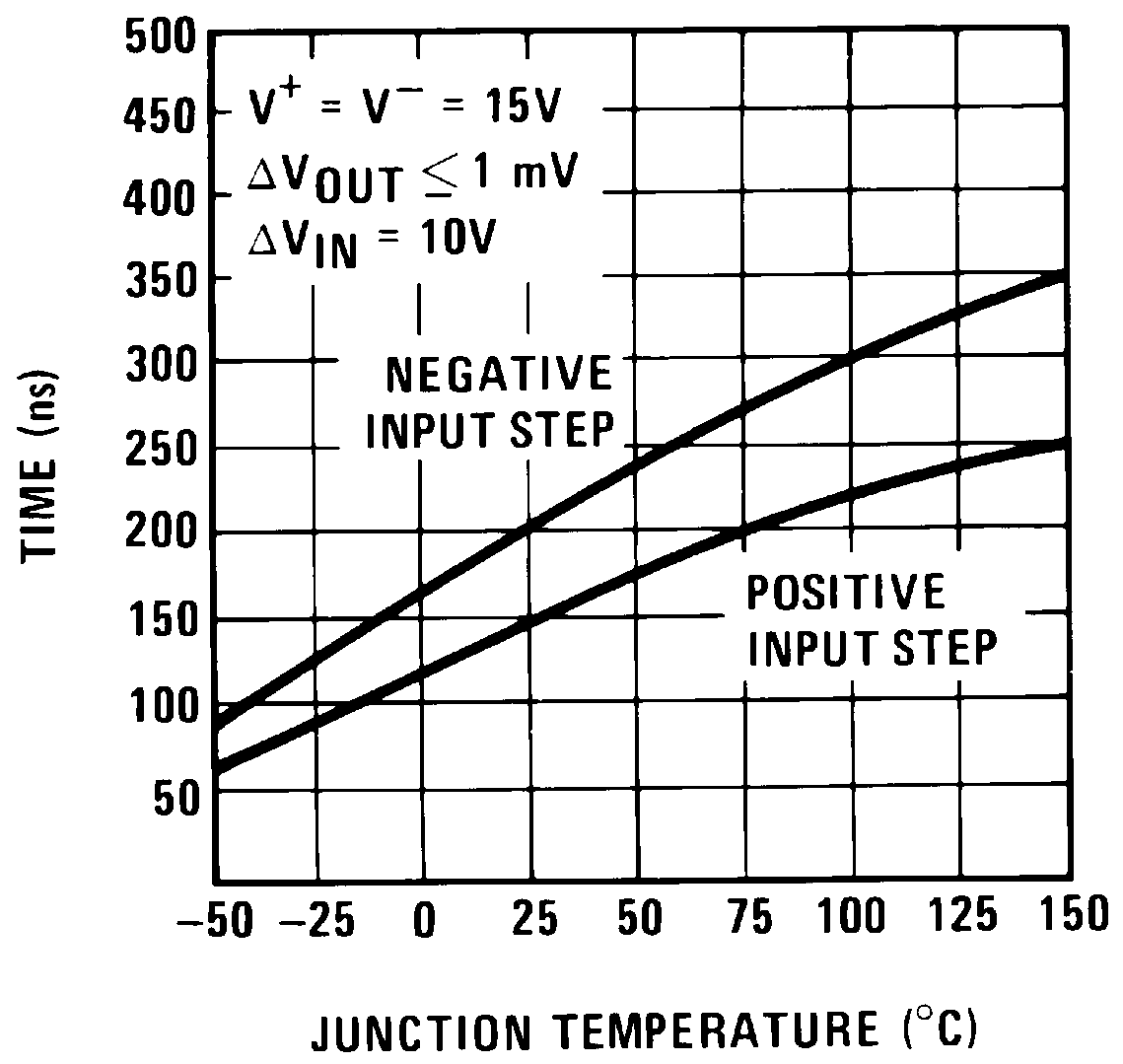 Figure 1. Aperture Time
 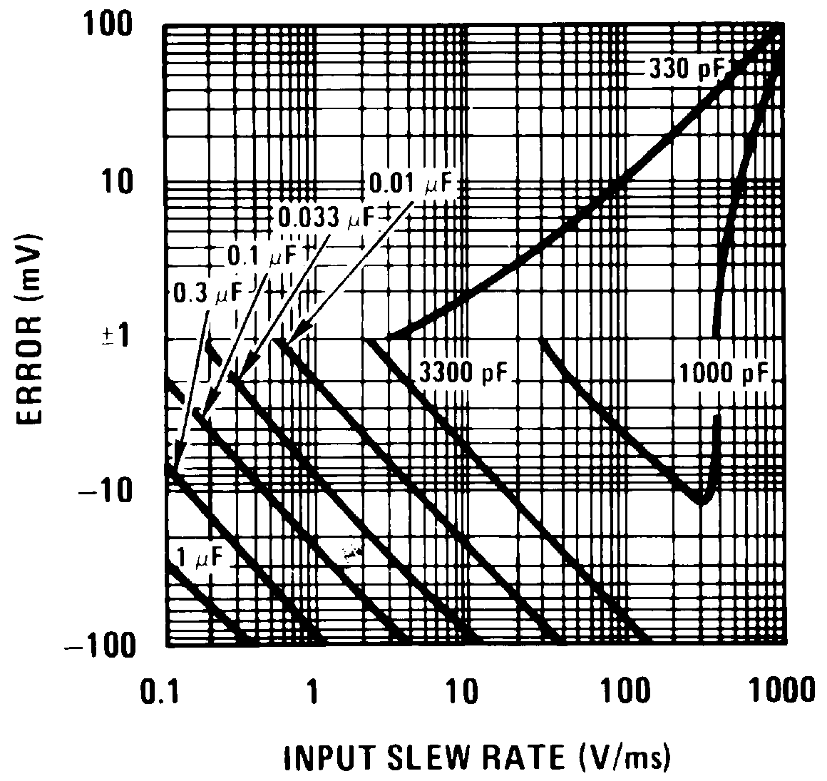 Figure 3. Dynamic Sampling Error
 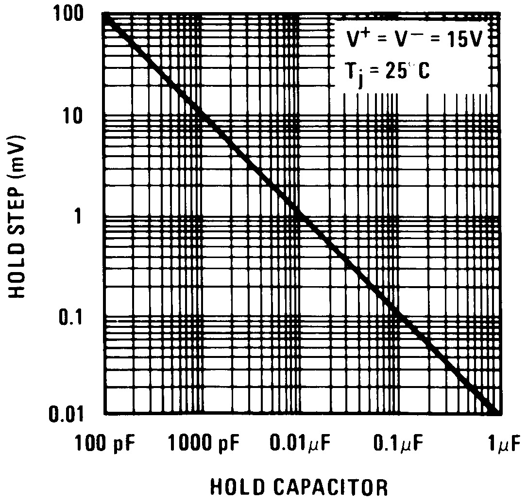 Figure 5. Hold Step
 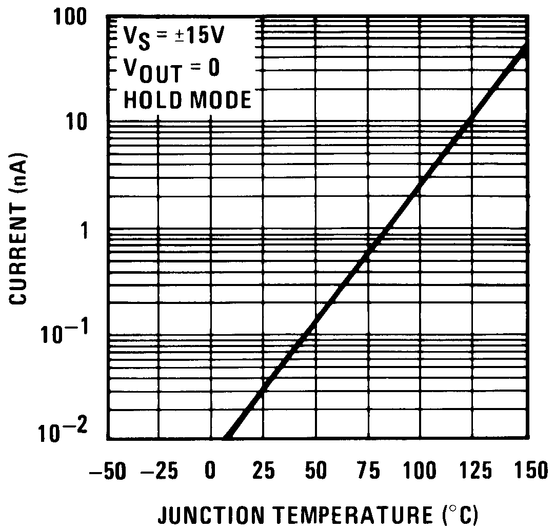 Figure 7. Leakage Current into Hold Capacitor
 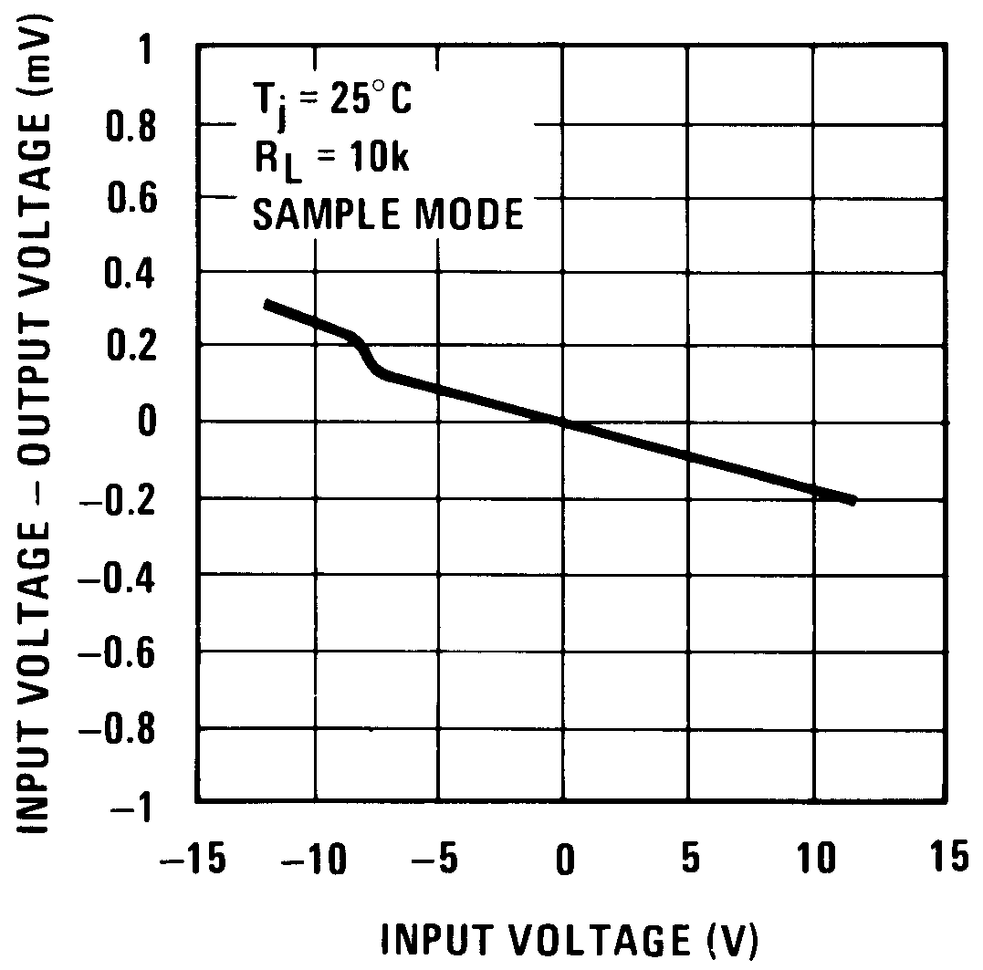 Figure 9. Gain Error
 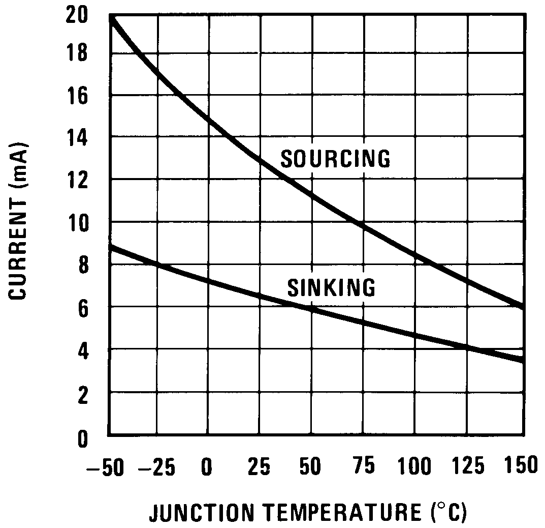 Figure 11. Output Short Circuit Current
 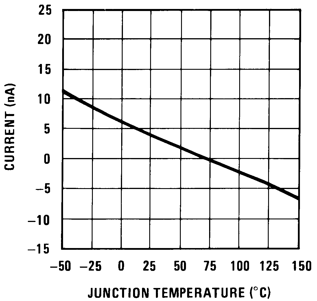 Figure 13. Input Bias Current
 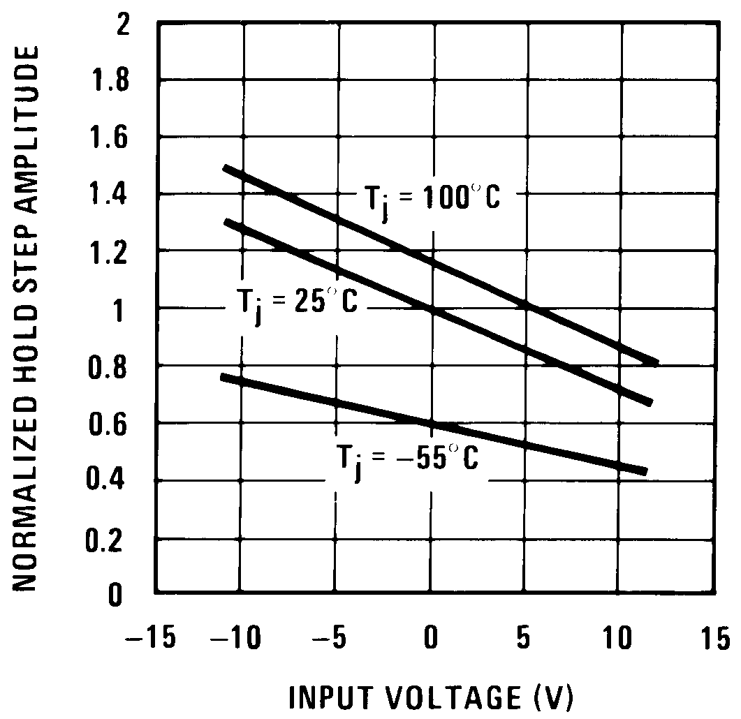 Figure 15. Hold Step vs Input Voltage
 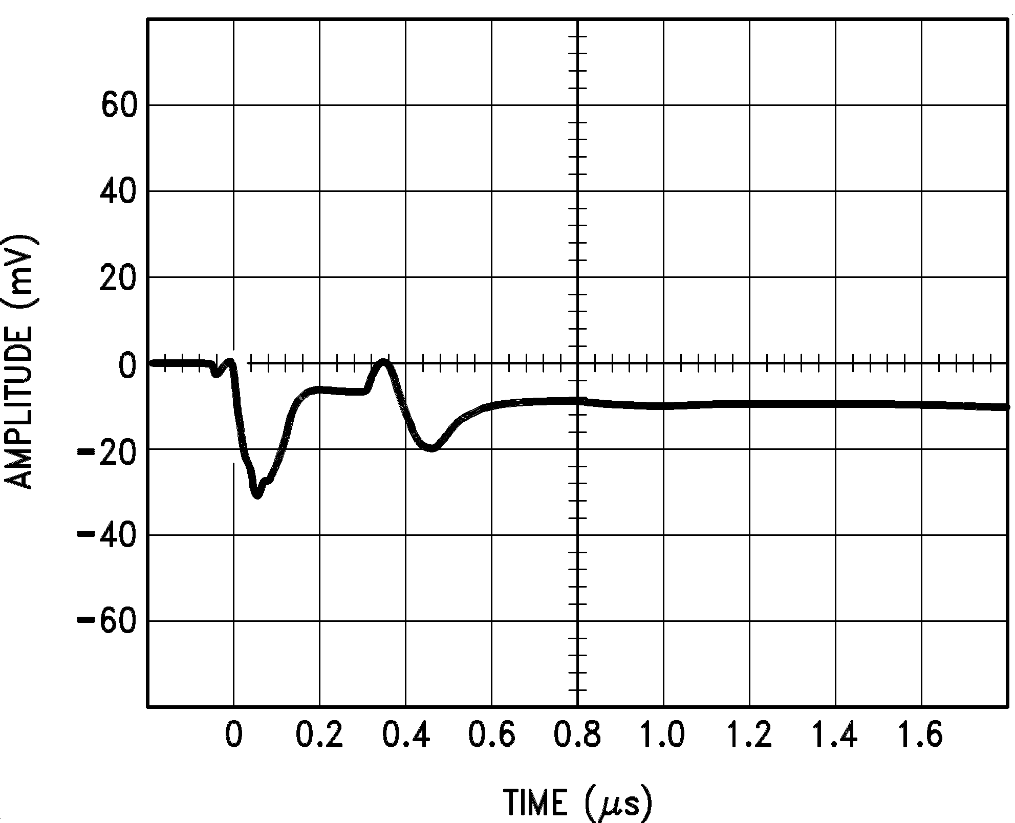 Figure 17. Output Transient at Start of Hold Mode
 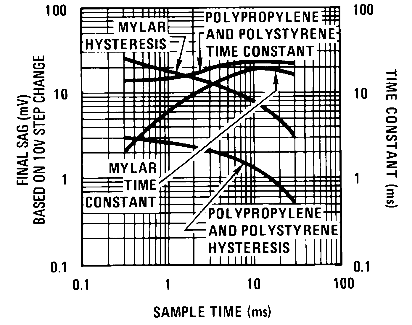 Figure 2. Dielectric Absorption Error in Hold Capacitor
 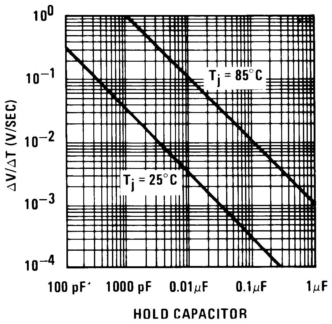 Figure 4. Output Droop Rate
 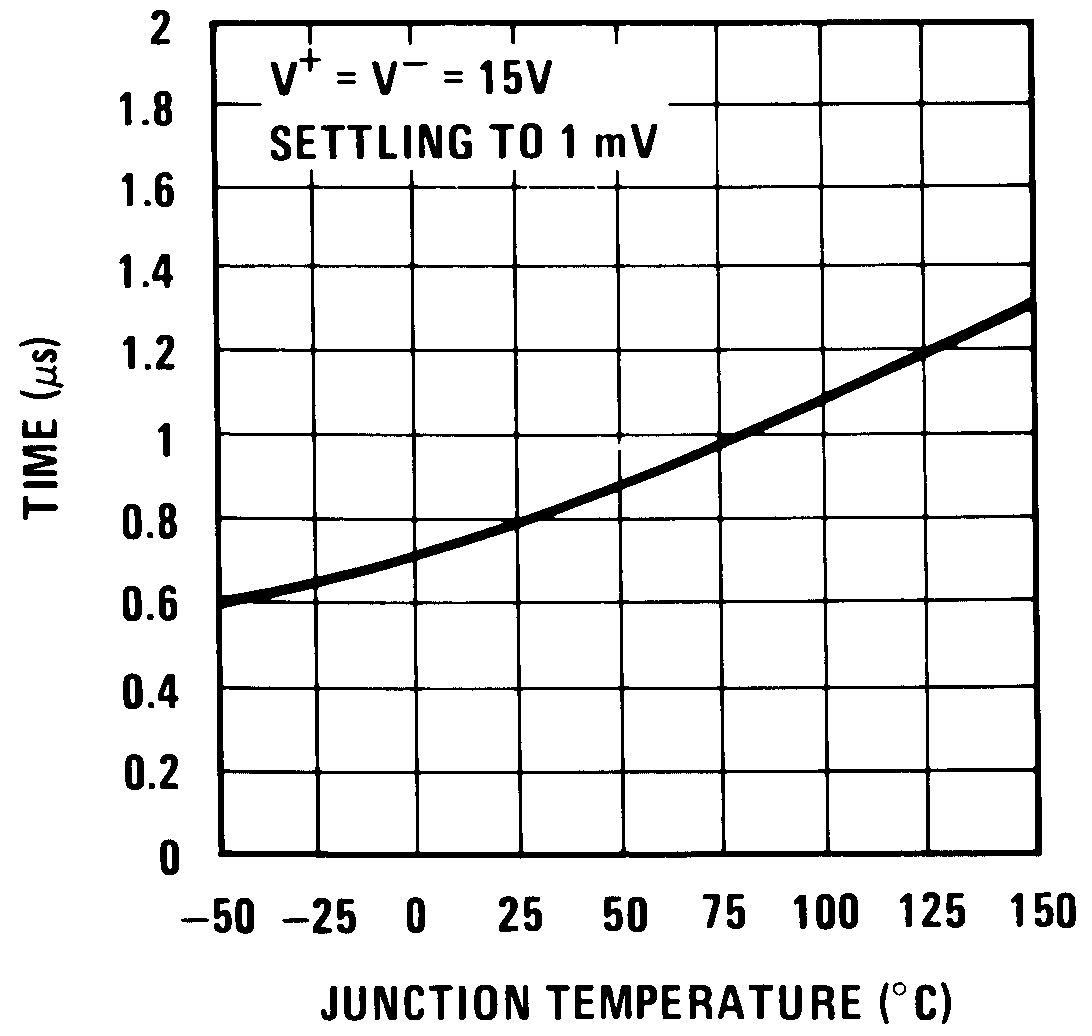 Figure 6. Hold Settling Time
 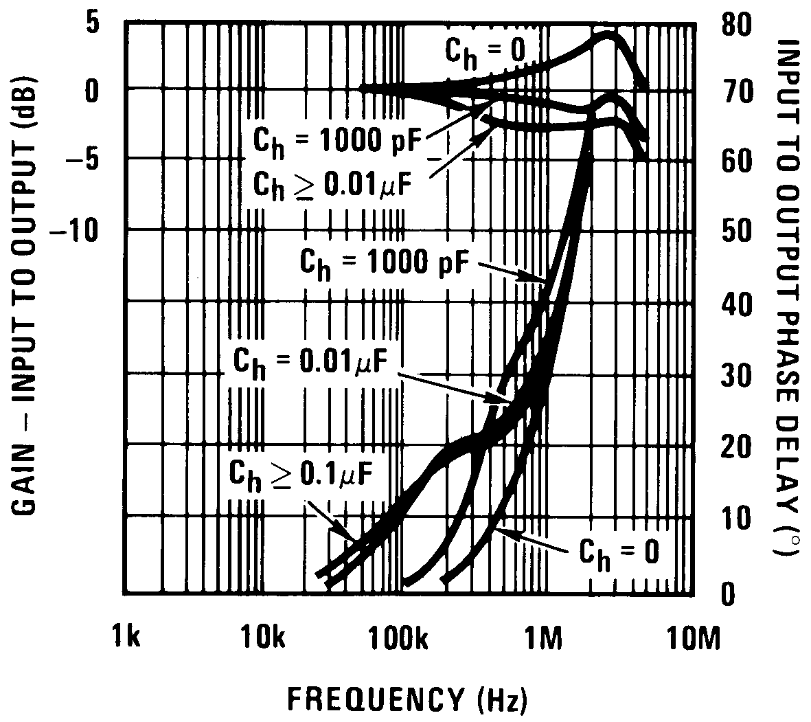 Figure 8. Phase and Gain (Input to Output, Small Signal)
 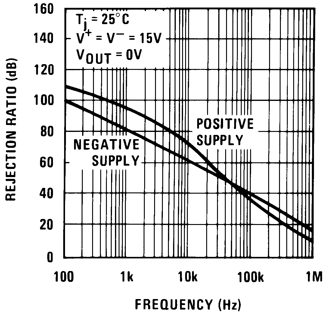 Figure 10. Power Supply Rejection
 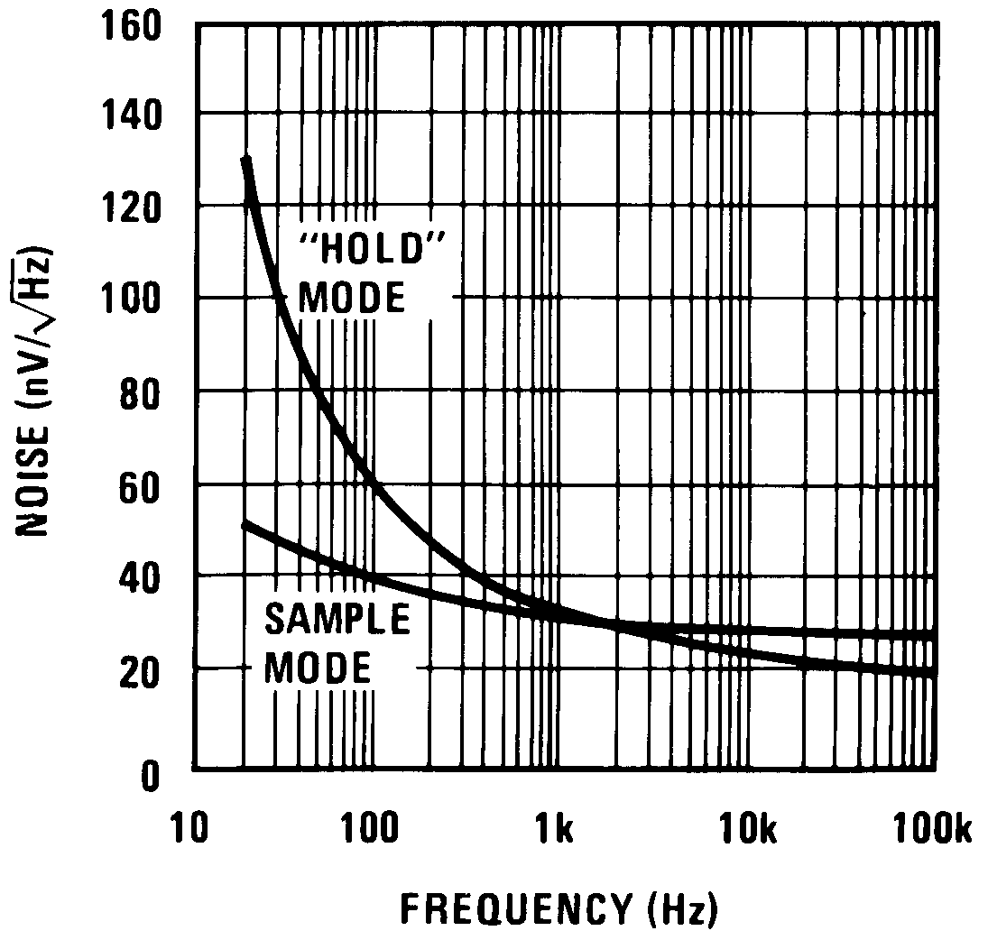 Figure 12. Output Noise
 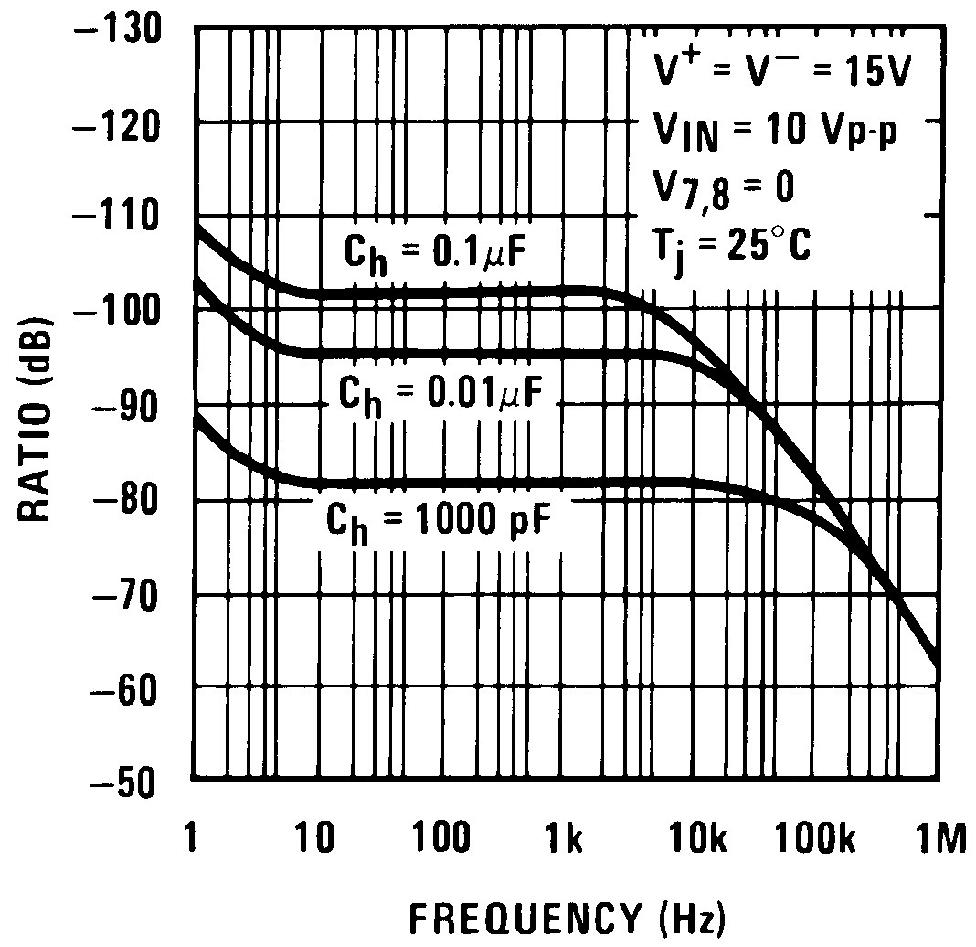 Figure 14. Feedthrough Rejection Ratio (Hold Mode)
 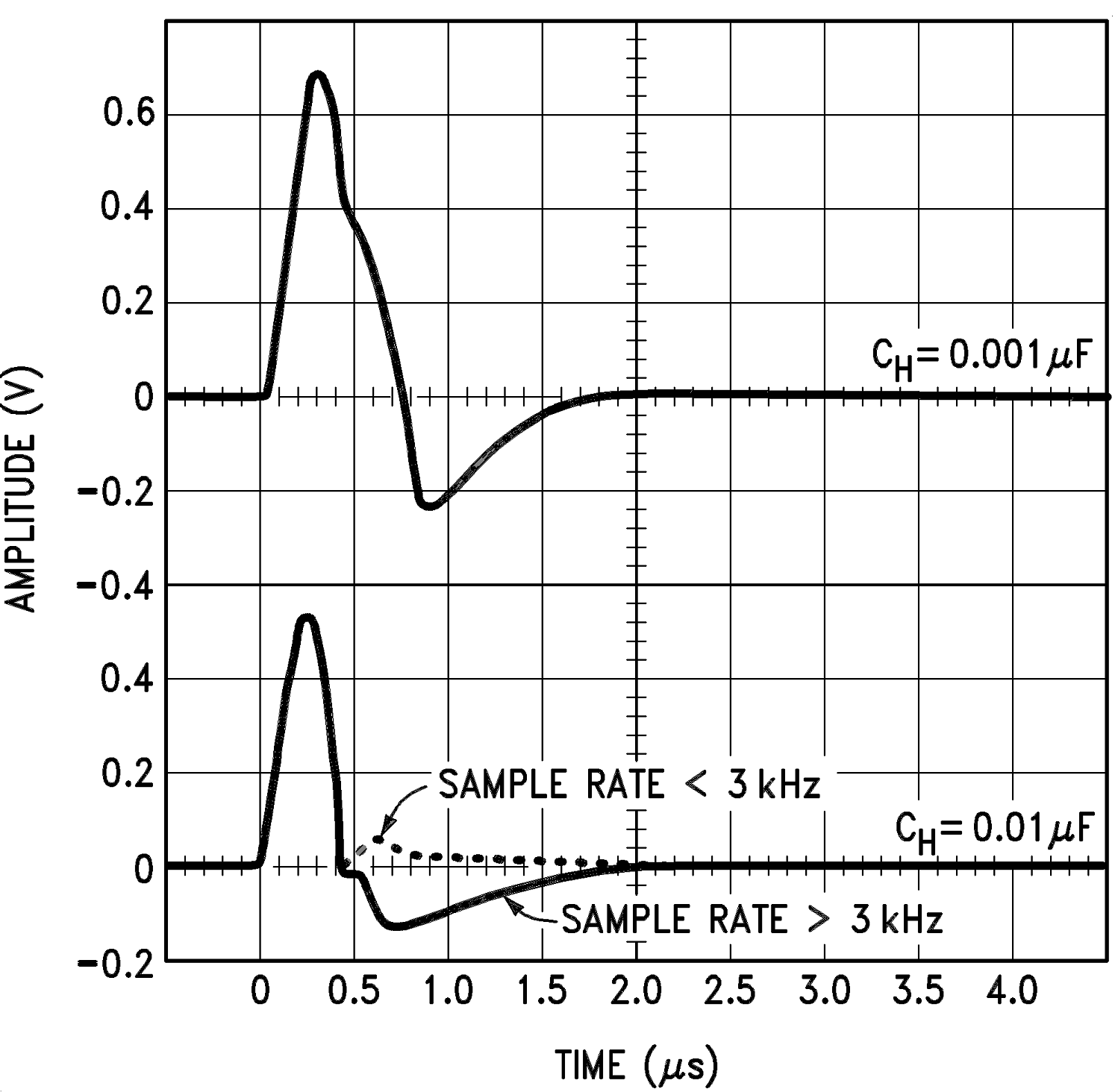 Figure 16. Output Transient at Start of Sample Mode