SLCS007K September   1973  – March 2017 LM111 , LM211 , LM311

PRODUCTION DATA.  

  1. Features
  2. Applications
  3. Description
  4. Revision History
  5. Pin Configuration and Functions
  6. Specifications
    1. 6.1 Absolute Maximum Ratings
    2. 6.2 ESD Ratings
    3. 6.3 Recommended Operating Conditions
    4. 6.4 Thermal Information (8-Pin Packages)
    5. 6.5 Thermal Information (20-Pin Package)
    6. 6.6 Electrical Characteristics
    7. 6.7 Switching Characteristics
    8. 6.8 Typical Characteristics
  7. Parameter Measurement Information
  8. Detailed Description
    1. 8.1 Overview
    2. 8.2 Functional Block Diagram
    3. 8.3 Feature Description
    4. 8.4 Device Functional Modes
      1. 8.4.1 Voltage Comparison
  9. Application and Implementation
    1. 9.1 Application Information
    2. 9.2 Typical Application
      1. 9.2.1 Design Requirements
      2. 9.2.2 Detailed Design Procedure
        1. 9.2.2.1 Input Voltage Range
        2. 9.2.2.2 Minimum Overdrive Voltage
        3. 9.2.2.3 Output and Drive Current
        4. 9.2.2.4 Response Time
      3. 9.2.3 Application Curves
    3. 9.3 System Examples
  10. 10Power Supply Recommendations
  11. 11Layout
    1. 11.1 Layout Guidelines
    2. 11.2 Layout Example
  12. 12Device and Documentation Support
    1. 12.1 Related Links
    2. 12.2 Receiving Notification of Documentation Updates
    3. 12.3 Community Resources
    4. 12.4 Trademarks
    5. 12.5 Electrostatic Discharge Caution
    6. 12.6 Glossary
  13. 13Mechanical, Packaging, and Orderable Information

Package Options

Refer to the PDF data sheet for device specific package drawings

Mechanical Data (Package|Pins)
  • FK|20
  • JG|8
Thermal pad, mechanical data (Package|Pins)
Orderable Information

Layout

Layout Guidelines

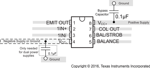
To create an accurate comparator application without hysteresis, maintain a stable power supply with minimized noise and glitches, which can affect the high level input common-mode voltage range. To achieve this accuracy, add a bypass capacitor between the supply voltage and ground. Place a bypass capacitor on the positive power supply and negative supply (if available).

Layout Example

LM111 LM211 LM311 lm311_layout.gif Figure 34. LMx11 Layout Example