SNVSAA9 October 2017 LM138QML
PRODUCTION DATA.
- 1 Features
- 2 Applications
- 3 Description
- 4 Revision History
- 5 Pin Configuration and Functions
- 6 Specifications
- 7 Detailed Description
- 8 Application and Implementation
- 9 Power Supply Recommendations
- 10Layout
- 11Device and Documentation Support
- 12Mechanical, Packaging, and Orderable Information
Package Options
Mechanical Data (Package|Pins)
- K|2
- Y|0
Thermal pad, mechanical data (Package|Pins)
Orderable Information
8 Application and Implementation
NOTE
Information in the following applications sections is not part of the TI component specification, and TI does not warrant its accuracy or completeness. TI’s customers are responsible for determining suitability of components for their purposes. Customers should validate and test their design implementation to confirm system functionality.
8.1 Application Information
In operation, the LM138QML device develops a nominal 1.25-V reference voltage, VREF, between the output and adjustment terminal. The reference voltage is impressed across program resistor R1 and, since the voltage is constant, a constant current I1 then flows through the output set resistor R2, giving an output voltage of:

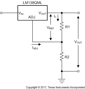
Because the 50-μA current from the adjustment terminal represents an error term, the LM138QML was designed to minimize IADJ and make it very constant with line and load changes. To do this, all quiescent operating current is returned to the output establishing a minimum load current requirement. If there is insufficient load on the output, the output rises.
8.2 Typical Applications
8.2.1 Constant 5-V Regulator
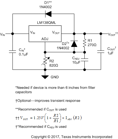 Figure 15. Constant 5-V Regulator
8.2.1.1 Design Requirements
Table 1. Design Parameters
| PARAMETER | PART NUMBER/VALUE | DESCRIPTION |
|---|---|---|
| Feedback resistor 1 (R1) | 270 Ω | The LM138QML produces a typical 1.24-V potential between the OUTPUT and ADJUST pins; therefore, placing a 270-Ω resistor between the OUTPUT and ADJUST pins causes 4.6 mA to flow through R1 and R2 |
| Feedback resistor 2 (R2) | 820 Ω | To achieve a 5-V output, the sum of the voltages across R1 and R2 must equal 5 V. Therefore, VR2 must equal 3.76 V when 4.6 mA is flowing through it. R2 = VR2 / I = 3.76 V / 4.6 mA = ~820 Ω. |
| Input capacitor (CIN) | 0.1 µF | 0.1 µF of input capacitance helps filter out unwanted noise, especially if the regulator is located far from the power supply filter capacitors. |
| Output capacitor (COUT) | 1 µF | The regulator is stable without any output capacitance, but adding a 1-µF capacitor improves the transient response. |
| Adjust capacitor (CADJ) | 10 µF | A 10-µF capacitor bypassing the ADJUST pin to ground improves the regulators ripple rejection. |
| Protection diode 1 (D1) | 1N4002 | Protection diode D1 is recommended if COUT is used. The diode provides a low-impedance discharge path to prevent the capacitor from discharging into the output of the regulator (see Protection Diodes). |
| Protection diode 2 (D2) | 1N4002 | Protection diode D2 is recommended if CADJ is used. The diode provides a low-impedance discharge path to prevent the capacitor from discharging into the output of the regulator (see Protection Diodes). |
8.2.1.2 Detailed Design Procedure
8.2.1.2.1 External Capacitors
An input bypass capacitor is recommended. A 0.1-μF disc or 1-μF solid tantalum on the input is suitable input bypassing for almost all applications. The device is more sensitive to the absence of input bypassing when adjustment or output capacitors are used but the above values will eliminate the possibility of problems.
The adjustment terminal can be bypassed to ground on the LM138QML to improve ripple rejection. This bypass capacitor prevents ripple from being amplified as the output voltage is increased. With a 10-μF bypass capacitor, 75-dB ripple rejection is obtainable at any output level. Increases over 20 μF do not appreciably improve the ripple rejection at frequencies above 120 Hz. If the bypass capacitor is used, it is sometimes necessary to include protection diodes to prevent the capacitor from discharging through internal low current paths and damaging the device.
In general, the best type of capacitors to use are solid tantalum. Solid tantalum capacitors have low impedance even at high frequencies. Depending upon capacitor construction, it takes about 25 μF in aluminum electrolytic to equal 1-μF solid tantalum at high frequencies. Ceramic capacitors are also good at high frequencies; however, some types have a large decrease in capacitance at frequencies around 0.5 MHz. For this reason, a 0.01-μF disc may seem to work better than a 0.1-μF disc as a bypass.
Although the LM138QML is stable with no output capacitors, like any feedback circuit, certain values of external capacitance can cause excessive ringing. This occurs with values between 500 pF and 5000 pF. A 1-μF solid tantalum (or 25-μF aluminum electrolytic) on the output swamps this effect and insures stability.
8.2.1.2.2 Load Regulation
The LM138QML device is capable of providing extremely good load regulation but a few precautions are needed to obtain maximum performance. The current set resistor connected between the adjustment terminal and the output terminal (usually 240 Ω) should be tied directly to the output of the regulator (case) rather than near the load; this eliminates line drops from appearing effectively in series with the reference and degrading regulation. For example, a 15-V regulator with 0.05-Ω resistance between the regulator and load will have a load regulation due to line resistance of 0.05 Ω × IL. If the set resistor is connected near the load the effective line resistance will be 0.05 Ω (1 + R2/R1) or in this case, 11.5 times worse.
Figure 16 shows the effect of resistance between the regulator and 240-Ω set resistor.
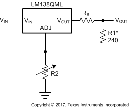 Figure 16. Regulator With Line Resistance in Output Lead
With the TO-3 package, it is easy to minimize the resistance from the case to the set resistor by using two separate leads to the case. The ground of R2 can be returned near the ground of the load to provide remote ground sensing and improve load regulation.
8.2.1.2.3 Protection Diodes
When external capacitors are used with any IC regulator, it is sometimes necessary to add protection diodes to prevent the capacitors from discharging through low current points into the regulator. Most 20-μF capacitors have low enough internal series resistance to deliver 20-A spikes when shorted. Although the surge is short, there is enough energy to damage parts of the IC.
When an output capacitor is connected to a regulator and the input is shorted, the output capacitor discharges into the output of the regulator. The discharge current depends on the value of the capacitor, the output voltage of the regulator, and the rate of decrease of VIN. In the LM138QML, this discharge path is through a large junction that is able to sustain 25-A surge with no problem; this is not true of other types of positive regulators. For output capacitors of 100 μF or less at an output of 15 V or less, there is no need to use diodes.
The bypass capacitor on the adjustment terminal can discharge through a low current junction. Discharge occurs when either the input or output is shorted. Internal to the LM138QML is a 50-Ω resistor which limits the peak discharge current. No protection is needed for output voltages of 25-V or less and 10-μF capacitance. Figure 17 shows an LM138QML with protection diodes included for use with outputs greater than 25 V and high values of output capacitance.
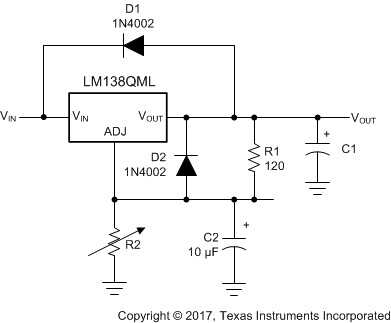
D2 protects against C2
 Figure 17. Regulator With Protection Diodes
8.2.1.3 Application Curves
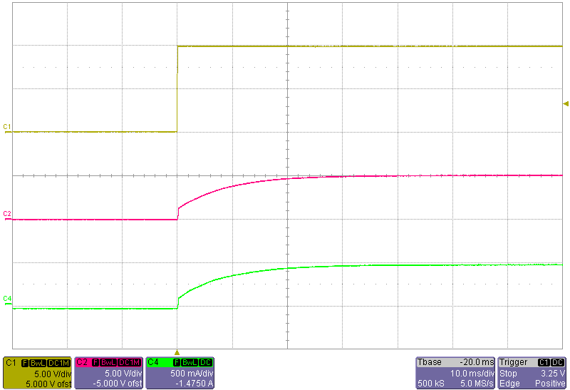 Figure 18. Regulator Start-Up
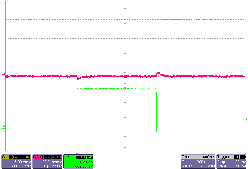 Figure 20. Regulator Response to Load Stop
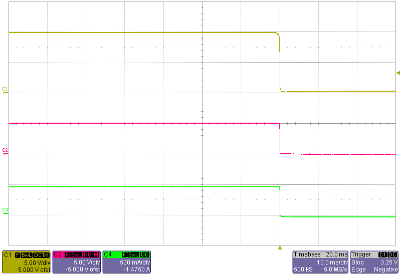 Figure 19. Regulator Shutdown
8.3 System Examples
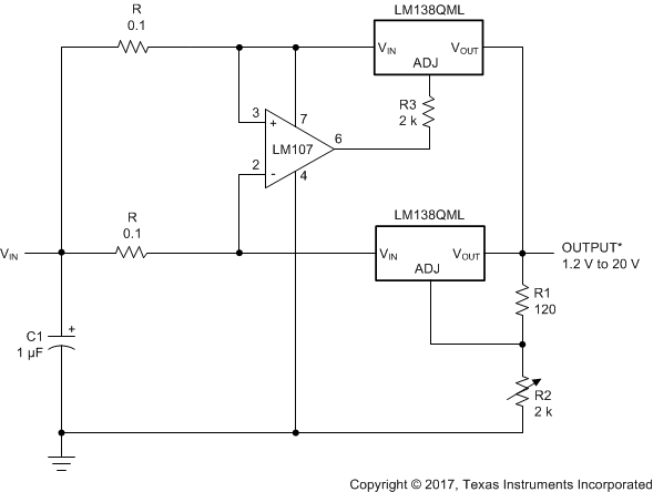
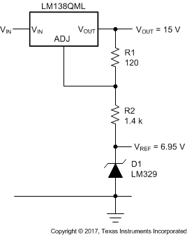 Figure 21. Regulator and Voltage Reference
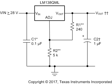
† Optional—improves transient response. Output capacitors in the range of 1 μF to 1000 μF of aluminum or tantalum electrolytic are commonly used to provide improved output impedance and rejection of transients.
* Needed if device is more than 6 inches from filter capacitors.

** R1, R2 as an assembly can be ordered from Bourns:
MIL part no. 7105A-AT2-502
COMM part no. 7105A-AT7-502
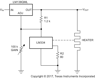 Figure 23. Temperature Controller
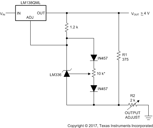
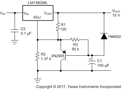 Figure 25. Slow Turnon 15-V Regulator
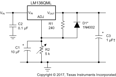
* Discharges C1 if output is shorted to ground
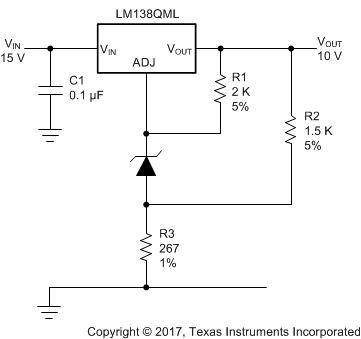 Figure 27. High Stability 10-V Regulator
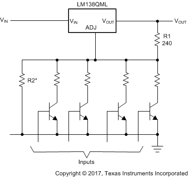
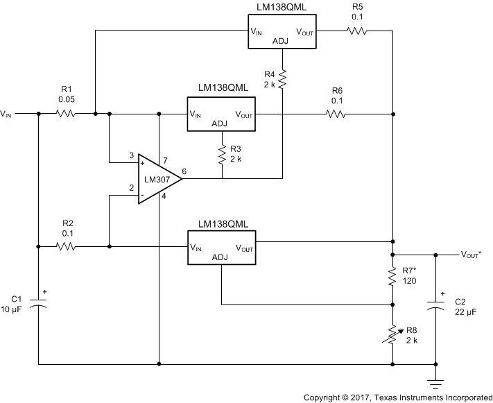
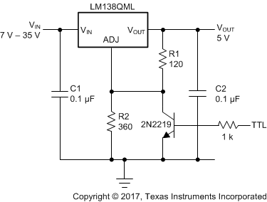
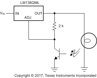 Figure 31. Light Controller
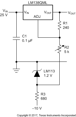
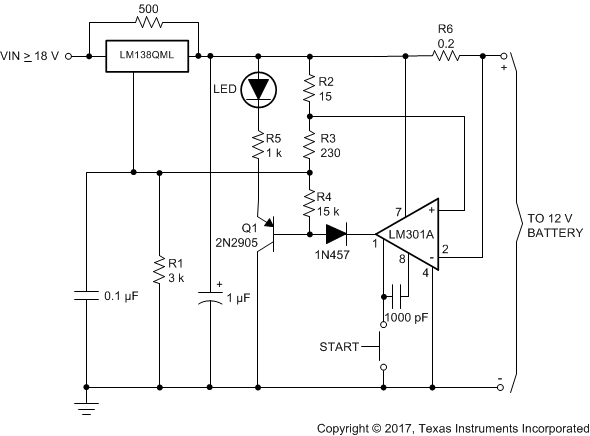 Figure 33. 12-V Battery Charger
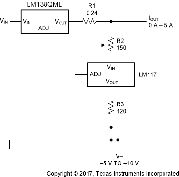 Figure 34. Adjustable Current Regulator
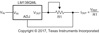 Figure 35. Precision Current Limiter
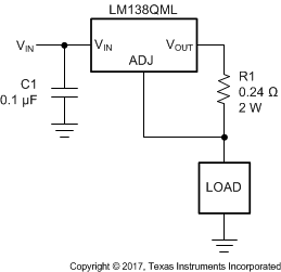 Figure 36. 5-A Current Regulator

* All outputs within ±100 mV
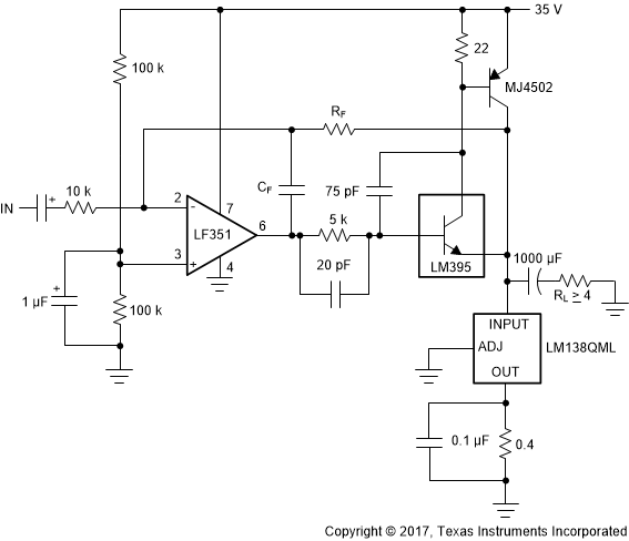
AV = 10, RF = 100k, CF = 10 pF
Bandwidth ≥ 100 kHz
Distortion ≤ 0.1%
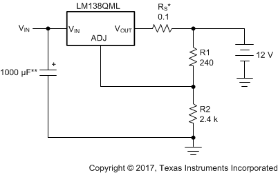

Use of RS allows low charging rates with fully charged battery.
** The 1000 μF is recommended to filter out input transients
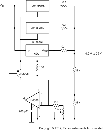 Figure 41. Adjustable 15-A Regulator
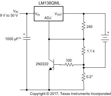
** The 1000 μF is recommended to filter out input transients.
