SNOSB87D March   2011  – May 2019 LM21215A

PRODUCTION DATA.  

  1. Features
  2. Applications
    1.     Efficiency at 2.5 V, 500 kHz
  3. Description
    1.     Typical Application Circuit
      1.      Device Images
  4. Revision History
  5. Pin Configuration and Functions
    1.     Pin Functions
  6. Specifications
    1. 6.1 Absolute Maximum Ratings
    2. 6.2 ESD Ratings
    3. 6.3 Recommended Operating Conditions
    4. 6.4 Thermal Information
    5. 6.5 Electrical Characteristics
    6. 6.6 Typical Characteristics
  7. Detailed Description
    1. 7.1 Overview
    2. 7.2 Functional Block Diagram
    3. 7.3 Feature Description
      1. 7.3.1 Precision Enable
      2. 7.3.2 Input Voltage UVLO
      3. 7.3.3 Soft-Start Capability
      4. 7.3.4 PGOOD Indicator
      5. 7.3.5 Frequency Synchronization
      6. 7.3.6 Current Limit
      7. 7.3.7 Short Circuit Protection
    4. 7.4 Device Functional Modes
      1. 7.4.1 Light-Load Operation
      2. 7.4.2 Overvoltage and Undervoltage Handling
      3. 7.4.3 Thermal Shutdown
  8. Application and Implementation
    1. 8.1 Application Information
    2. 8.2 Typical Applications
      1. 8.2.1 Typical Application 1
        1. 8.2.1.1 Design Requirements
        2. 8.2.1.2 Detailed Design Procedure
          1. 8.2.1.2.1 Custom Design With WEBENCH® Tools
          2. 8.2.1.2.2 Output Voltage Setpoint
          3. 8.2.1.2.3 Precision Enable
          4. 8.2.1.2.4 Filter Inductor Selection
          5. 8.2.1.2.5 Output Capacitor Selection
          6. 8.2.1.2.6 Input Capacitor Selection
          7. 8.2.1.2.7 Control Loop Compensation
        3. 8.2.1.3 Application Curves
      2. 8.2.2 Typical Application 2
        1. 8.2.2.1 Design Requirements
        2. 8.2.2.2 Detailed Design Procedure
  9. Power Supply Recommendations
  10. 10Layout
    1. 10.1 Layout Guidelines
      1. 10.1.1 Compact PCB Layout for EMI Reduction
      2. 10.1.2 Thermal Design
      3. 10.1.3 Ground Plane Design
    2. 10.2 Layout Example
  11. 11Device and Documentation Support
    1. 11.1 Device Support
      1. 11.1.1 Third-Party Products Disclaimer
      2. 11.1.2 Development Support
        1. 11.1.2.1 Custom Design With WEBENCH® Tools
    2. 11.2 Documentation Support
      1. 11.2.1 Related Documentation
    3. 11.3 Community Resources
    4. 11.4 Trademarks
    5. 11.5 Electrostatic Discharge Caution
    6. 11.6 Glossary
  12. 12Mechanical, Packaging, and Orderable Information

Package Options

Mechanical Data (Package|Pins)
Thermal pad, mechanical data (Package|Pins)
Orderable Information

Current Limit

The LM21215A has overcurrent protection to avoid excessive current levels through the power MOSFETs and inductor. A current limit condition exists when the high-side MOSFET's current exceeds the rising current limit level, ICLR. The control circuitry responds to this event by turning off the high-side MOSFET and turning on the low-side MOSFET. This forces a negative voltage on the inductor, thereby causing the inductor current to decrease. The high-side MOSFET does not conduct again until the lower current limit level, ICLF, is sensed on the low-side MOSFET. At this point, the LM21215A resumes normal switching.

A current limit condition causes the internal soft-start voltage to ramp downward. After the internal soft-start ramps below the feedback (FB) voltage, nominally 0.6 V, FB begins to ramp downward, as well. This voltage foldback limits the power consumption in the device during a sustained overload. After the current limit condition is cleared, the internal soft-start voltage ramps up again. Figure 26 describes current limit behavior including VSS, VFB, VOUT and VSW waveforms.
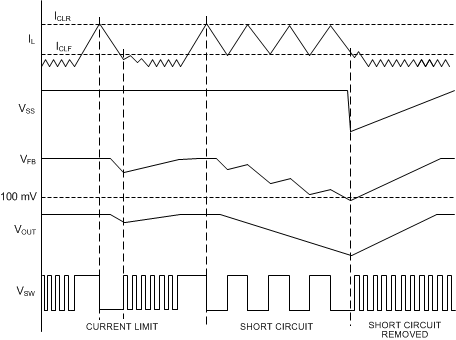
LM21215A current_limit_nosb87.gifFigure 26. Current Limit Conditions