SNVS654J February 2010 – December 2015 LM25066
PRODUCTION DATA.
- 1 Features
- 2 Applications
- 3 Description
- 4 Revision History
- 5 Description (continued)
- 6 Pin Configuration and Functions
- 7 Specifications
-
8 Detailed Description
- 8.1 Overview
- 8.2 Functional Block Diagram
- 8.3 Feature Description
- 8.4 Device Functional Modes
- 8.5
Register Maps
- 8.5.1
PMBus Command Support
- 8.5.1.1
Standard PMBus™ Commands
- 8.5.1.1.1 OPERATION (01h)
- 8.5.1.1.2 CLEAR_FAULTS (03h)
- 8.5.1.1.3 CAPABILITY (19h)
- 8.5.1.1.4 VOUT_UV_WARN_LIMIT (43h)
- 8.5.1.1.5 OT_FAULT_LIMIT (4Fh)
- 8.5.1.1.6 OT_WARN_LIMIT (51h)
- 8.5.1.1.7 VIN_OV_WARN_LIMIT (57h)
- 8.5.1.1.8 VIN_UV_WARN_LIMIT (58h)
- 8.5.1.1.9 STATUS_BYTE (78h)
- 8.5.1.1.10 STATUS_WORD (79h)
- 8.5.1.1.11 STATUS_VOUT (7Ah)
- 8.5.1.1.12 STATUS_INPUT (7Ch)
- 8.5.1.1.13 STATUS_TEMPERATURE (7Dh)
- 8.5.1.1.14 STATUS_CML (7Eh)
- 8.5.1.1.15 STATUS_MFR_SPECIFIC (80h)
- 8.5.1.1.16 READ_VIN (88h)
- 8.5.1.1.17 READ_VOUT (8Bh)
- 8.5.1.1.18 READ_TEMPERATURE_1 (8Dh)
- 8.5.1.1.19 MFR_ID (99h)
- 8.5.1.1.20 MFR_MODEL (9Ah)
- 8.5.1.1.21 MFR_REVISION (9Bh)
- 8.5.1.2
Manufacturer Specific PMBus™ Commands
- 8.5.1.2.1 MFR_SPECIFIC_00: READ_VAUX (D0h)
- 8.5.1.2.2 MFR_SPECIFIC_01: MFR_READ_IIN (D1h)
- 8.5.1.2.3 MFR_SPECIFIC_02: MFR_READ_PIN (D2h)
- 8.5.1.2.4 MFR_SPECIFIC_03: MFR_IN_OC_WARN_LIMIT (D3h)
- 8.5.1.2.5 MFR_SPECIFIC_04: MFR_PIN_OP_WARN_LIMIT (D4h)
- 8.5.1.2.6 MFR_SPECIFIC_05: READ_PIN_PEAK (D5h)
- 8.5.1.2.7 MFR_SPECIFIC_06: CLEAR_PIN_PEAK (D6h)
- 8.5.1.2.8 MFR_SPECIFIC_07: GATE_MASK (D7h)
- 8.5.1.2.9 MFR_SPECIFIC_08: ALERT_MASK (D8h)
- 8.5.1.2.10 MFR_SPECIFIC_09: DEVICE_SETUP (D9h)
- 8.5.1.2.11 MFR_SPECIFIC_10: BLOCK_READ (DAh)
- 8.5.1.2.12 MFR_SPECIFIC_11: SAMPLES_FOR_AVG (DBh)
- 8.5.1.2.13 MFR_SPECIFIC_12: READ_AVG_VIN (DCh)
- 8.5.1.2.14 MFR_SPECIFIC_13: READ_AVG_VOUT (DDh)
- 8.5.1.2.15 MFR_SPECIFIC_14: READ_AVG_IIN (DEh)
- 8.5.1.2.16 MFR_SPECIFIC_15: READ_AVG_PIN (DFh)
- 8.5.1.2.17 MFR_SPECIFIC_16: BLACK_BOX_READ (E0h)
- 8.5.1.2.18 MFR_SPECIFIC_17: READ_DIAGNOSTIC_WORD (E1h)
- 8.5.1.2.19 MFR_SPECIFIC_18: AVG_BLOCK_READ (E2h)
- 8.5.1.3 Reading and Writing Telemetry Data and Warning Thresholds
- 8.5.1.4 Determining Telemetry Coefficients Empirically With Linear Fit
- 8.5.1.5 Writing Telemetry Data
- 8.5.1.6 PMBus™ Address Lines (ADR0, ADR1, ADR2)
- 8.5.1.7 SMBA Response
- 8.5.1.1
Standard PMBus™ Commands
- 8.5.1
PMBus Command Support
-
9 Application and Implementation
- 9.1 Application Information
- 9.2
Typical Application
- 9.2.1
12-V, 45-A PMBus Hotswap Design
- 9.2.1.1 Design Requirements
- 9.2.1.2
Detailed Design Procedure
- 9.2.1.2.1 Select RSNS and CL Setting
- 9.2.1.2.2 Selecting the Hotswap FETs
- 9.2.1.2.3 Select Power Limit
- 9.2.1.2.4 Set Fault Timer
- 9.2.1.2.5 Check MOSFET SOA
- 9.2.1.2.6 Switching to dV/dt based Start-up
- 9.2.1.2.7 Choosing the VOUT Slew Rate
- 9.2.1.2.8 Select Power Limit and Fault Timer
- 9.2.1.2.9 Set Undervoltage and Overvoltage Threshold
- 9.2.1.2.10 Power Good Pin
- 9.2.1.2.11 Input and Output Protection
- 9.2.1.2.12 Final Schematic and Component Values
- 9.2.2 Application Curves
- 9.2.1
12-V, 45-A PMBus Hotswap Design
- 10Power Supply Recommendations
- 11Layout
- 12Device and Documentation Support
- 13Mechanical, Packaging, and Orderable Information
Package Options
Mechanical Data (Package|Pins)
- NHZ|24
Thermal pad, mechanical data (Package|Pins)
Orderable Information
9 Application and Implementation
NOTE
Information in the following applications sections is not part of the TI component specification, and TI does not warrant its accuracy or completeness. TI’s customers are responsible for determining suitability of components for their purposes. Customers should validate and test their design implementation to confirm system functionality.
9.1 Application Information
The LM25066 is a hot swap with a PMBus interface that provides current, voltage, power, and status information to the host. As a hot swap, it is used to manage inrush current and protect in case of faults.
When designing a hot swap, three key scenarios should be considered:
- Start-up
- Output of a hot swap is shorted to ground while the hot swap is on. This is often referred to as a hot-short.
- Powering-up a board when the output and ground are shorted. This is usually called a start-into-short.
All of these scenarios place a lot of stress on the hot swap MOSFET and thus special care is required when designing the hot swap circuit to keep the MOSFET operating within its SOA (Safe Operating Area). Detailed design examples are provided in the following sections. Solving all of the equations by hand is cumbersome and can result in errors. Instead, TI recommends using the LM25066 Design Calculator provided in Development Support.
9.2 Typical Application
9.2.1 12-V, 45-A PMBus Hotswap Design
This section describes the design procedure for a 12-V, 45-A PMBus hot swap design.
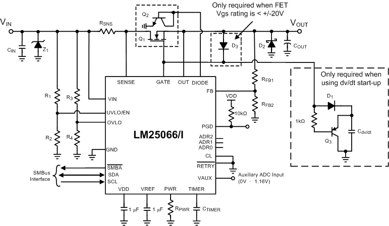 Figure 38. Typical Application Circuit
9.2.1.1 Design Requirements
Table 44 below summarizes the design parameters that must be known before designing a hot swap circuit. When charging the output capacitor through the hot swap MOSFET, the FET’s total energy dissipation equals the total energy stored in the output capacitor (1/2 CV2). Thus both the input voltage and Output capacitance will determine the stress experienced by the MOSFET. The maximum load current will drive the current limit and sense resistor selection. In addition, the maximum load current, maximum ambient temperature, and the thermal properties of the PCB (RθCA) will drive the selection of the MOSFET RDSON and the number of MOSFETs used. RθCA is a strong function of the layout and the amount of copper that is connected to the drain of the MOSFET. Note that the drain is not electrically connected to the ground plane and thus the ground plane cannot be used to help with heat dissipation. For this design example RθCA = 30 °C/W is used, which is similar to the LM25066 EVM. It’s a good practice to measure the RθCA of a given design after the physical PCBs are available.
Finally, it’s important to understand what test conditions the hot swap needs to pass. In general, a hot swap is designed to pass both a “Hot-Short” and a “Start into a Short”, which are described in the previous section. Also it is recommended to keep the load OFF until the hot swap is fully powered up. Starting the load early will cause unnecessary stress on the MOSFET and could lead to MOSFET failures or a failure to start-up.
Table 44. Design Parameters
| PARAMETER | EXAMPLE VALUE |
|---|---|
| Input voltage range | 10 V to 14 V |
| Maximum load current | 45 A |
| Maximum output capacitance of the hotswap | 5600 µF |
| Maximum ambient temperature | 55°C |
| MOSFET RθCA (function of layout) | 30°C/W |
| Pass hot-short on output? | Yes |
| Pass a start into short? | Yes |
| Is the load off until PG asserted? | Yes |
| Can a hot board be plugged back in? | Yes |
9.2.1.2 Detailed Design Procedure
9.2.1.2.1 Select RSNS and CL Setting
LM25066 can be used with a VCL of 25 mV or 46 mV. In general using the 25-mV threshold will result in a lower RSNS and lower I2R losses. This option is selected for this design by connecting the CL pin directly to VDD. It is recommended to target a current limit that is at least 10% above the maximum load current to account for the tolerance of the LM25066 current limit. Targeting a current limit of 50 A the sense resistor can be calculated using Equation 5:

Typically sense resistors are only available in discrete values. If a precise current limit is desired, a sense resistor along with a resistor divider can be used as shown in Figure 39.
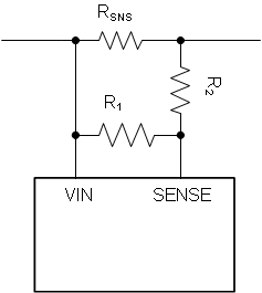 Figure 39. SENSE Resistor Divider
If using a resistor divider, then the next larger available sense resistor should be chosen (1 mΩ for example). The ratio of R1 and R2 can then be calculated using Equation 6:

Note that the SENSE pin will pull 25 μA of current, which will create an offset across R2. It is recommended to keep R2 below 10 Ω to reduce the offset that this introduces. In addition the 1% resistors will add to the current monitoring error. Finally, if the resistor divider approach is used, the user should compute the effective sense resistance (RSNS,EFF) using Equation 7 and use that in all equations instead of RSNS.

Note that for many applications, a precise current limit may not be required. In that case, it’s simpler to pick the next smaller available sense resistor. For this application, a 0.5-mΩ resistor can be used for a 50 A current limit.
9.2.1.2.2 Selecting the Hotswap FETs
It is critical to select the correct MOSFET for a hot swap design. The device must meet the following requirements:
- The VDS rating should be sufficient to handle the maximum system voltage along with any ringing caused by transients. For most 12-V systems a 30-V FET is a good choice.
- The SOA of the FET should be sufficient to handle all usage cases: start-up, hot-short, start into short.
- RDSON should be sufficiently low to maintain the junction and case temperature below the maximum rating of the FET. In fact, it is recommended to keep the steady state FET temperature below 125°C to allow margin to handle transients.
- Maximum continuous current rating should be above the maximum load current and the pulsed drain current must be greater than the current threshold of the circuit breaker. Most MOSFETs that pass the first three requirements will also pass these two.
- A VGS rating of ± 20 V is required, because the LM25066 can pull up the gate as high as 16 V above source.
- Otherwise, a diode (D3 in Figure 38) can be used to protect MOSFETs with a ± 12 V VGS rating.
For this design the CSD17556Q5B was selected for its low RDSON and good SOA. After selecting the MOSFET, the maximum steady state case temperature can be calculated using Equation 8:

Note that the RDSON is a strong function of junction temperature, which for most MOSFETs will be close to the case temperature. A few iterations of the above equations may be necessary to converge on the final RDSON and TC,MAX value. According to the CSD17556Q5B datasheet, its RDSON is approximately 1.3x at 85°C. Equation 9 uses this RDSON value to compute the TC,MAX.

This maximum steady state case temperature indicates that a second MOSFET may be needed to reduce and distribute power dissipation during normal operation. When using parallel MOSFETs, the maximum steady state case temperature can be calculated using Equation 10:

Thus using two of the CSD17556Q5B in parallel will result in a steady state temperature of:

Note that the computed TC,MAX is close to the junction temperature assumed for RDSON. Thus no further iterations are necessary.
9.2.1.2.3 Select Power Limit
In general, a lower power limit setting is preferred to reduce the stress on the MOSFET. However, when the LM25066 is set to a very low power limit setting, it has to regulate the FET current and hence the voltage across the sense resistor (VSNS) to a very low value. VSNS can be calculated using Equation 12:

To avoid significant degradation of the power limiting a VSNS of less than 4 mV is not recommended. Based on this requirement the minimum allowed power limit can be calculated using Equation 13:

In most applications the power limit can be set to PLIM,MIN using Equation 14. Here RSNS and RPWR are in Ωs and PLIM is in Watts.

So note that the minimum RPWR would occur when VDS = VIN,MAX. We can then calculate the minimum RPWR using Equation 15:

The next largest available resistor should be selected. In this case a 5.23-kΩ resistor was chosen, which sets a 112.72 W power limit.
9.2.1.2.4 Set Fault Timer
The fault timer runs when the hot swap is in power limit or current limit, which is the case during start-up. Thus the timer has to be sized large enough to prevent a time-out during start-up. If the device starts directly into current limit (ILIM) × VDS < PLIM) the maximum start time can be calculated using Equation 16:

For most designs (including this example) ILIM × VDS > PLIM so the hot swap will start in power limit and transition into current limit. In that case the estimated start time can be calculated using Equation 17:

Note that the above start-time assumes constant, typical current limit and power limit values. The actual start-up time will be slightly longer, as the power limit is a function of VDS and will decrease as the output voltage increases. To ensure that the timer never times out during start-up, it is recommended to set the fault time (tflt) to be 2 × tstart or 10.06 ms. This will account for the variation in power limit, timer current, and timer capacitance. Thus CTIMER can be calculated using Equation 18:

The next largest available CTIMER is chosen as 560 nF. Once the CTIMER is chosen the actual programmed fault time can be calculated using Equation 19:

9.2.1.2.5 Check MOSFET SOA
Once the power limit and fault timer are chosen, it’s critical to check that the FET will stay within its SOA during all test conditions. During a “Hot-Short” the circuit breaker will trip and the LM25066 will restart into power limit until the timer runs out. In the worst case the MOSFET’s VDS will equal VIN,MAX, IDS will equal PLIM / VIN,MAX and the stress event will last for tflt. For this design example the MOSFET will have 14 V, 8 A across it for 10.58 ms.
Based on the SOA of the CSD17556Q5B, it can handle 14 V, 10 A for 10 ms and it can handle 14 V, 3 A for
100 ms. The SOA for 10.58 ms can be extrapolated by approximating SOA vs time as a power function as shown in Equation 20 through Equation 23:


Note that the SOA of a MOSFET is specified at a case temperature of 25°C, while the case temperature can be much hotter during a hot-short. The SOA should be de-rated based on TC,MAX using Equation 24:

Based on this calculation the MOSFET can handle 5.24 A, 14 V for 10.58 ms at elevated case temperature, but is required to handle 8 A during a hot-short. This means the MOSFET will be at risk of getting damaged during a hot-short. In general, it is recommended for the MOSFET to be able to handle a minimum of 1.3x more power than what is required during a hot-short in order to provide margin to cover the variance of the power limit and fault time.
9.2.1.2.6 Switching to dV/dt based Start-up
For designs with large load currents and output capacitances, using a power limit based start-up can be impractical. Fundamentally, increasing load currents will reduce the sense resistor, which will increase the minimum power limit. Using a larger output capacitor will result in a longer start-up time and require a longer fault timer. Thus a longer fault timer and a larger power limit setting are required, which places more stress on the MOSFET during a hot-short or a start into short. Eventually, there will be no FETs that can support such a requirement.
To avoid this problem, a dV/dt limiting capacitor (CdV/dt) can be used to limit the slew rate of the gate and the output voltage. The inrush current can be set arbitrarily small by reducing the slew rate of the VOUT. In addition, the power limit is set to satisfy the minimum power limit requirement and to keep the timer from running during start-up (make PLIM / VIN,MAX > IINR). Since the timer doesn’t run during start-up it can be made small to reduce the stress that the MOSFET experiences during a start into short or a hot-short.
The D2 prevents the charge of CdV/dt from interfering with the power limit loop during a hot-short event and Q3 discharges CdV/dt when the hot swap gate comes down.
9.2.1.2.7 Choosing the VOUT Slew Rate
The inrush current should be kept low enough to keep the MOSFET within its SOA during start-up. Note that the total energy dissipated in the MOSFET during start-up is constant regardless of the inrush time. Thus, stretching it out over a longer time will always reduce the stress on the MOSFET as long as the load is off during start-up.
When choosing a target slew rate, one should pick a reasonable number, check the SOA and reduce the slew rate if necessary. Using 0.25 V/ms as a starting point the inrush current can be computed as follows:

Assuming a maximum input voltage of 14 V, it will take 56 ms to start-up. Note that the power dissipation of the FET will start at VIN,MAX × IINR and reduce to zero as the VDS of the MOSFET is reduced. Note that the SOA curves assume the same power dissipation for a given time. A conservative approach is to assume an equivalent power profile where PFET = VIN,MAX × IINR for t = tstart-up /2. In this instance, the SOA can be checked by looking at a 14 V, 1.4 A, 28 ms pulse. Using the same technique as Check MOSFET SOA, the MOSFET SOA can be estimated with Equation 26.

This value has to also be derated for temperature. For this calculation, it is assumed that TC can equal TA,MAX when the board is plugged in. This would occur if a board is plugged in at an elevated ambient temperature environment.

Based on this calculation the MOSFET can handle 4.44 A, 14 V for 28 ms at elevated ambient temperature, and is required to handle 1.4 A. This indicates the MOSFET will stay well-within its SOA during a start-up if the slew rate is 0.25 V/ms or less. Note that if the load is off during start-up, the total energy dissipated in the FET is constant regardless of the slew rate. Thus a lower slew rate will always place less stress on the FET. To ensure that the slew rate is at most 0.25 V/ms the CdV/dt should be chosen with Equation 28.

The next largest available CdV/dt is chosen to be 100 nF. Then the typical slew rate and start time can be computed to be 0.22 V/ms as shown below, making the typical start time 55 ms, assuming 12 V input.

In certain applications, TC,MAX may be used for temperature derating instead. This would only occur if a hot board is unplugged and then plugged back in before it cools off to ambient temperature. This is worst case and for many applications, the TA,MAX can be used for this derating.

Based on this calculation using TC,MAX for derating, the MOSFET can handle 3.15 A, 14 V for 28 ms at elevated case temperature, and is required to handle 1.4 A. This indicates the MOSFET will stay well-within its SOA during a start-up if the slew rate is 0.25 V/ms or less.
9.2.1.2.8 Select Power Limit and Fault Timer
When picking the power limit, it needs to meet 2 requirements:
- Power limit is large enough to avoid operating with VSNS < 4 mV
- Power limit is large enough to ensure that the timer doesn’t run during start up. Picking a power limit such that it is 2x of IINR,MAX × VIN,MAX is good practice.
Thus the minimum allowed power limit can be computed with Equation 31.

Next, the power limit is set to PLIM,MIN using the equation below. Here RSNS and RPWR are in Ωs and PLIM is in Watts.

The closest available resistor should be selected. In this case a 5.23-kΩ resistor was chosen.
Next a fault timer value should be selected. In general, the timer value should be decreased until there is enough margin between available SOA and the power pulse the FET experiences during a hot-short. For this design a 22-nF CTIMER was chosen corresponding to a 420-µs fault time. The available SOA is extrapolated using the method described earlier.


Next the available SOA is derated for temperature:

Note that only 4 A was required, while the FET can support 17.17A. This confirms that the design will be robust and have plenty of margin.
9.2.1.2.9 Set Undervoltage and Overvoltage Threshold
By programming the UVLO and OVLO thresholds the LM25066 enables the series pass device (Q1) when the input supply voltage (VSYS) is within the desired operational range. If VSYS is below the UVLO threshold, or above the OVLO threshold, Q1 is switched off, denying power to the load. Hysteresis is provided for each threshold.
9.2.1.2.9.1 Option A
The configuration shown in Figure 40 requires three resistors (R1-R3) to set the thresholds.
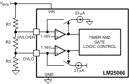 Figure 40. UVLO and OVLO Thresholds Set By R1-R3
The procedure to calculate the resistor values is as follows:
- Choose the upper UVLO threshold (VUVH), and the lower UVLO threshold (VUVL).
- Choose the upper OVLO threshold (VOVH).
- The lower OVLO threshold (VOVL) cannot be chosen in advance in this case, but is determined after the values for R1-R3 are determined. If VOVL must be accurately defined in addition to the other three thresholds, see Option B below. The resistors are calculated as follows:


The lower OVLO threshold is calculated from:

As an example, assume the application requires the following thresholds: VUVH = 8 V, VUVL = 7 V, VOVH = 15 V.


The lower OVLO threshold calculates to 12.03 V and the OVLO hysteresis is 2.97 V. Note that the OVLO hysteresis is always slightly greater than the UVLO hysteresis in this configuration. When the R1-R3 resistor values are known, the threshold voltages and hysteresis are calculated from the following:


9.2.1.2.9.2 Option B
If all four thresholds must be accurately defined, the configuration in Figure 41 can be used.
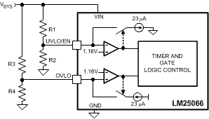 Figure 41. Programming the Four Thresholds
The four resistor values are calculated as follows:
- Choose the upper and lower UVLO thresholds (VUVH) and (VUVL).
- Choose the upper and lower OVLO threshold (VOVH) and (VOVL).


As an example, assume the application requires the following thresholds: VUVH = 8 V, VUVL = 7 V, VOVH = 15.5 V, and VOVL = 14 V. Therefore VUV(HYS) = 1 V and VOV(HYS) = 1.5 V. The resistor values are:
When the R1-R4 resistor values are known, the threshold voltages and hysteresis are calculated from the following:


9.2.1.2.9.3 Option C
The minimum UVLO level is obtained by connecting the UVLO/EN pin to VIN as shown in Figure 42. Q1 is switched on when the VIN voltage reaches the POR threshold (≊ 2.6 V). The OVLO thresholds are set using R3, R4. Their values are calculated using the procedure in Option B.
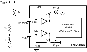 Figure 42. UVLO = POR
9.2.1.2.9.4 Option D
The OVLO function can be disabled by grounding the OVLO pin. The UVLO thresholds are set as described in Option B or Option C.
For this design example option B is used and the following values are targeted: VUVH = 10 V, VUVL = 9 V, VOVH = 15 V, VOVL = 14 V. R1, R2, R3, and R4 are computed using the equations below:


Nearest available 1% resistors should be chosen. Set R1 = 43.2 kΩ, R2 = 6.49 kΩ, R3 = 43.2 kΩ, and R4 = 3.65 kΩ.
9.2.1.2.10 Power Good Pin
When the voltage at the FB pin increases above its threshold, the internal pulldown acting on the PGD pin is disabled allowing PGD to rise to VPGD through the pullup resistor, RPG, as shown in Figure 44. The pullup voltage (VPGD) can be as high as 17 V, and can be higher or lower than the voltages at VIN and OUT. VDD is a convenient choice for VPGD as it allows interface to low voltage logic and avoids glitching on PGD during power-up. If a delay is required at PGD, suggested circuits are shown in Figure 45. In Figure 45A capacitor CPG adds delay to the rising edge, but not to the falling edge. In Figure 45B, the rising edge is delayed by RPG1 + RPG2 and CPG, while the falling edge is delayed a lesser amount by RPG2 and CPG. Adding a diode across RPG2 (Figure 45C) allows for equal delays at the two edges, or a short delay at the rising edge and a long delay at the falling edge.
Setting the output threshold for the PGD pin requires two resistors (R4, R5) as shown in Figure 43. While monitoring the output voltage is shown in Figure 43, R4 can be connected to any other voltage which requires monitoring.
The resistor values are calculated as follows:
Choose the upper and lower threshold (VPGDH) and (VPGDL) at VOUT.

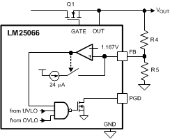 Figure 43. Programming the PGD Threshold
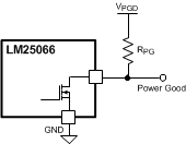 Figure 44. Power Good Output
 Figure 45. Adding Delay to the Power Good Output Pin
For this example PGDH of 9.25 V and PGDL of 8.75 V is targeted. R5 and R6 are computed using the equations below:


Nearest available 1% resistors should be chosen. Set R5 = 10 kΩ and R6 = 1.5 kΩ.
9.2.1.2.11 Input and Output Protection
Proper operation of the LM25066 hot swap circuit requires a voltage clamping element present on the supply side of the connector into which the hot swap circuit is plugged in. A TVS is ideal, as depicted in Figure 46. The TVS is necessary to absorb the voltage transient generated whenever the hot swap circuit shuts off the load current. This effect is the most severe during a hot-short when a large current is suddenly interrupted when the FET shuts off. The TVS should be chosen to have minimal leakage current at VIN,MAX and to clamp the voltage to under 24 V during hot-short events. For many high power applications, 5.0SMDJ13A is a good choice.
If the load powered by the LM25066 hot swap circuit has inductive characteristics, a Schottky diode is required across the LM25066's output, along with some load capacitance. The capacitance and the diode are necessary to limit the negative excursion at the OUT pin when the load current is shut off.
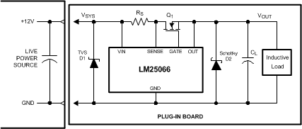 Figure 46. Output Diode Required for Inductive Loads
9.2.1.2.12 Final Schematic and Component Values
Figure 38 shows the schematic used to implement the requirements described in the previous section. In addition, Table 45 provides the final component values that were used to meet the design requirements for a
12-V, 45-A hot swap design. The application curves in the next section are based on these component values.
Table 45. Final Component Values (12-V, 45-A Design)
| COMPONENT | VALUE | |
|---|---|---|
| RSNS | 0.5 mΩ | |
| R1, R3 | 43.2 kΩ | |
| R2 | 6.49 kΩ | |
| R4 | 3.65 kΩ | |
| RFB1 | 10 kΩ | |
| RFB2 | 1.5 kΩ | |
| RPWR | 5.11 kΩ | |
| Q1 | CSD17556Q5B | |
| Q2 | MMBT3904 | |
| Q3 | MMBT3906 | |
| D1, D3 | 1N4148W-7-F | |
| D2 | SK153-TP | |
| Z1 | 5.0MDJA15A | |
| CdV/dt | 100 nF | |
| CTIMER | 22 nF | |
9.2.2 Application Curves
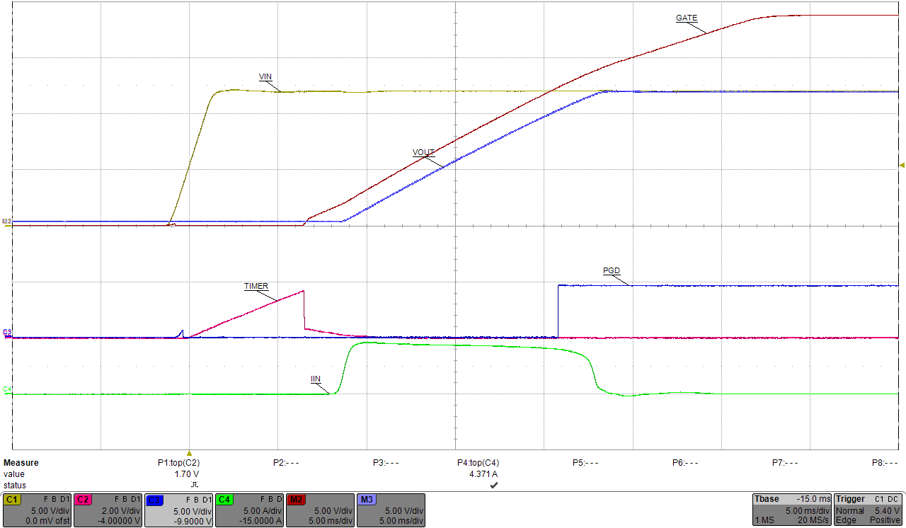
| VIN = 12 V |
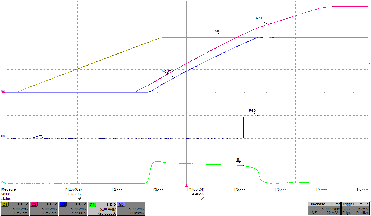 Figure 49. Undervoltage
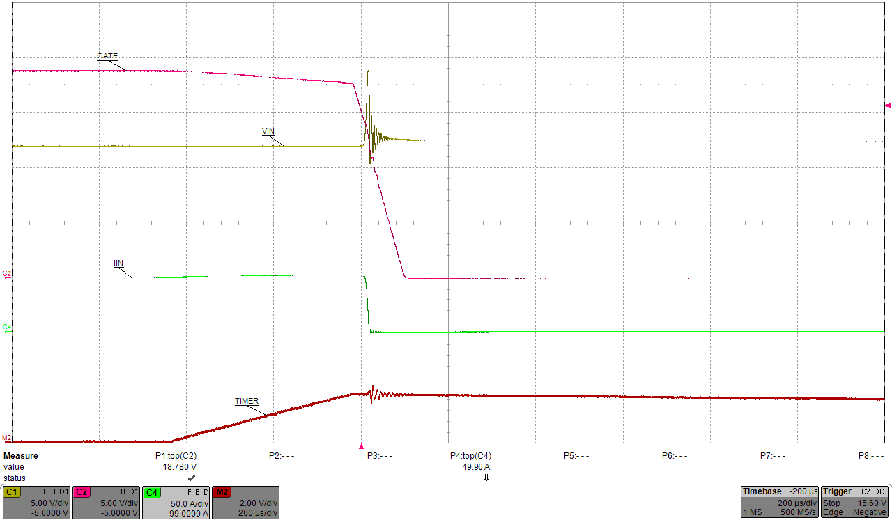 Figure 51. Gradual Overcurrent
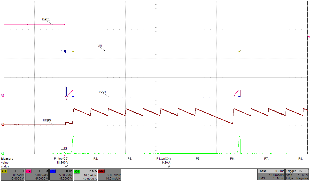 Figure 53. Hot Short on Vout (Zoomed Out)
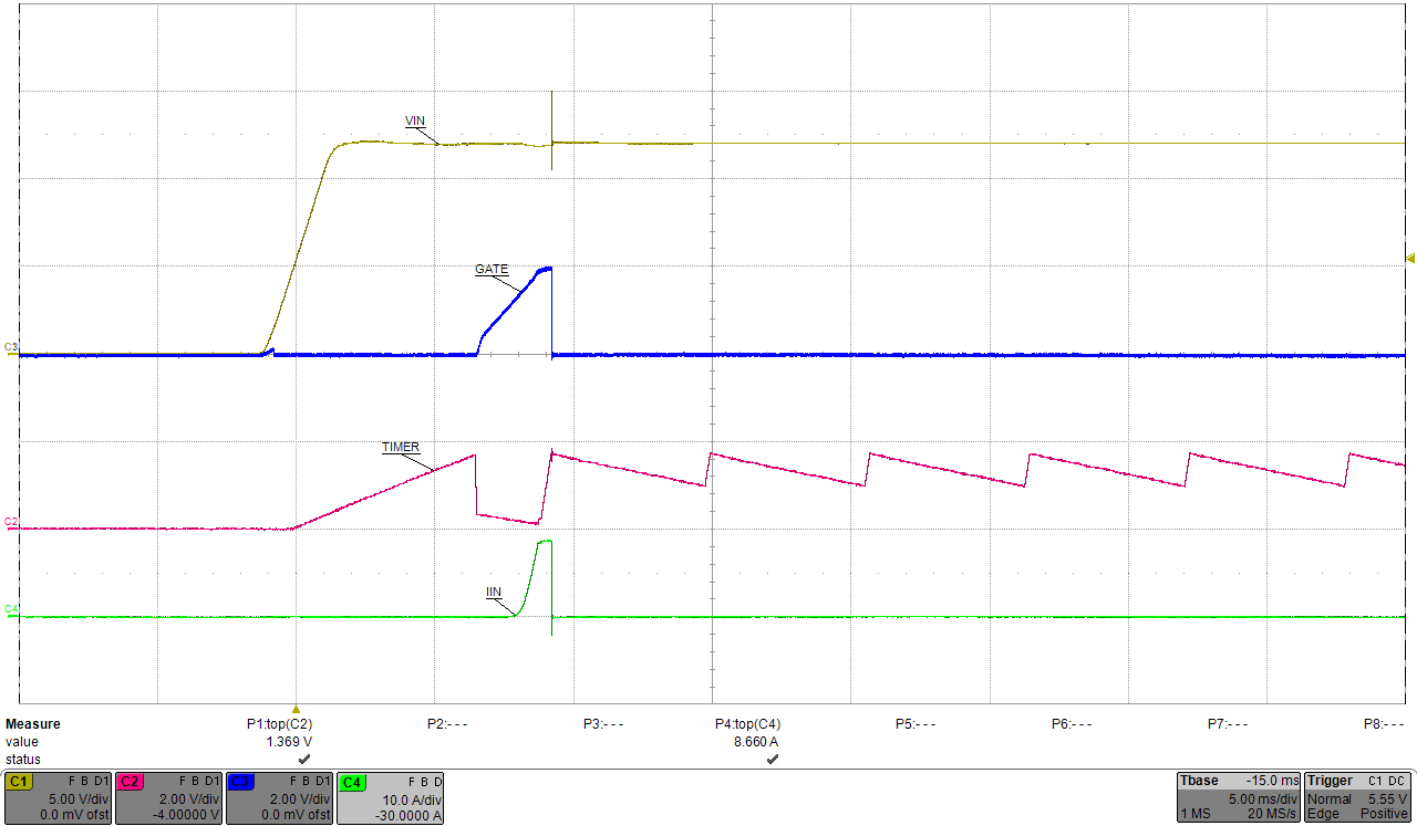
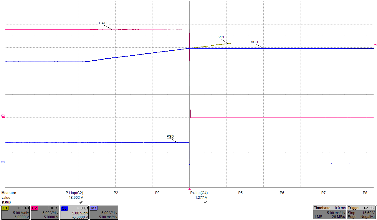 Figure 50. Overvoltage
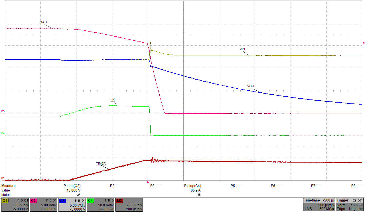 Figure 52. Loadstep
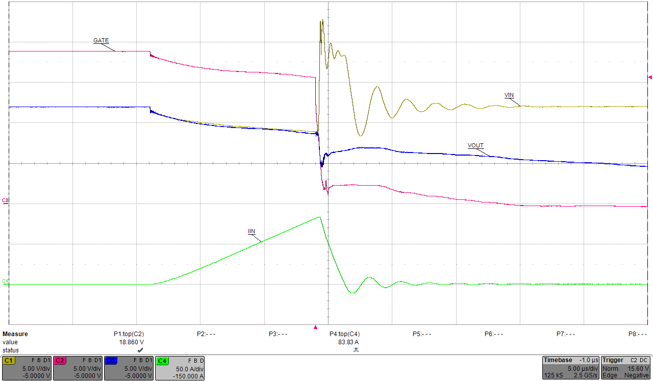 Figure 54. Hotshort on Vout (Zoomed In)