SNVS593J October 2008 – November 2014 LM25085 , LM25085-Q1
PRODUCTION DATA.
- 1 Features
- 2 Applications
- 3 Description
- 4 Revision History
- 5 Pin Configuration and Functions
- 6 Specifications
- 7 Detailed Description
- 8 Application and Implementation
- 9 Power Supply Recommendations
- 10Layout
- 11Device and Documentation Support
- 12Mechanical, Packaging, and Orderable Information
Package Options
Mechanical Data (Package|Pins)
Thermal pad, mechanical data (Package|Pins)
Orderable Information
10 Layout
10.1 Layout Guidelines
In most applications, the heat sink pad or tab of Q1 is connected to the switch node, i.e. the junction of Q1, L1 and D1. While it is common to extend the PC board pad from under these devices to aid in heat dissipation, the pad size should be limited to minimize EMI radiation from this switching node. If the PC board layout allows, a similarly sized copper pad can be placed on the underside of the PC board, and connected with as many vias as possible to aid in heat dissipation.
The voltage regulation, over-voltage, and current limit comparators are very fast and can respond to short duration noise pulses. Layout considerations are therefore critical for optimum performance. The layout must be as neat and compact as possible with all the components as close as possible to their associated pins. Two major current loops conduct currents which switch very fast, requiring the loops to be as small as possible to minimize conducted and radiated EMI. The first loop is that formed by CIN, Q1, L1, COUT, and back to CIN. The second loop is that formed by D1, L1, COUT, and back to D1. The connection from the anode of D1 to the ground end of CIN must be short and direct. CIN must be as close as possible to the VIN and GND pins, and CVCC must be as close as possible to the VIN and VCC pins.
If the anticipated internal power dissipation of the LM25085 will produce excessive junction temperatures during normal operation, a package option with an exposed pad must be used (HVSSOP-PowerPAD-8 or WSON-8). Effective use of the PC board ground plane can help dissipate heat. Additionally, the use of wide PC board traces, where possible, helps conduct heat away from the IC. Judicious positioning of the PC board within the end product, along with the use of any available air flow (forced or natural convection) also helps reduce the junction temperature.
10.2 Layout Example
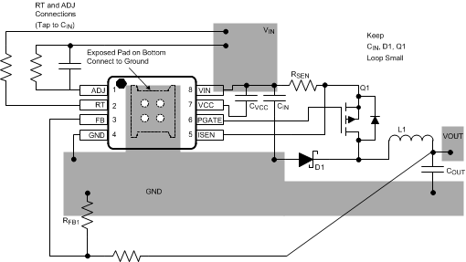 Figure 32. LM25085 Buck Converter Layout Example