SNVSAX7 June 2017 LM25118-Q1
PRODUCTION DATA.
- 1 Features
- 2 Applications
- 3 Description
- 4 Revision History
- 5 Pin Configuration and Functions
- 6 Specifications
- 7 Detailed Description
-
8 Application and Implementation
- 8.1 Application Information
- 8.2
Typical Application
- 8.2.1 Design Requirements
- 8.2.2
Detailed Design Procedure
- 8.2.2.1 Custom Design With WEBENCH® Tools
- 8.2.2.2 R7 = RT
- 8.2.2.3 Inductor Selection - L1
- 8.2.2.4 R13 = RSENSE
- 8.2.2.5 C15 = CRAMP
- 8.2.2.6 Inductor Current Limit Calculation
- 8.2.2.7 C9 - C12 = Output Capacitors
- 8.2.2.8 D1
- 8.2.2.9 D4
- 8.2.2.10 C1 - C5 = Input Capacitors
- 8.2.2.11 C20
- 8.2.2.12 C8
- 8.2.2.13 C16 = CSS
- 8.2.2.14 R8, R9
- 8.2.2.15 R1, R3, C21
- 8.2.2.16 R2
- 8.2.2.17 Snubber
- 8.2.2.18 Error Amplifier Configuration
- 8.2.3 Application Curves
- 9 Power Supply Recommendations
- 10Layout
- 11Device and Documentation Support
- 12Mechanical, Packaging, and Orderable Information
Package Options
Mechanical Data (Package|Pins)
- PWP|20
Thermal pad, mechanical data (Package|Pins)
- PWP|20
Orderable Information
9 Power Supply Recommendations
9.1 Bias Power Dissipation Reduction
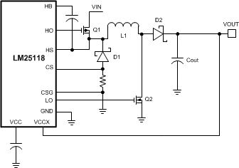
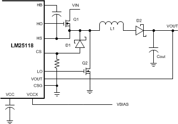
Buck or Buck-boost regulators operating with high-input voltage can dissipate an appreciable amount of power while supplying the required bias current of the IC. The VCC regulator must step-down the input voltage VIN to a nominal VCC level of 7 V. The large voltage drop across the VCC regulator translates into high power dissipation in the VCC regulator. There are several techniques that can significantly reduce this bias regulator power dissipation. Figure 27 and Figure 28 depict two methods to bias the IC, one from the output voltage and one from a separate bias supply. In the first case, the internal VCC regulator is used to initially bias the VCC pin. After the output voltage is established, the VCC pin bias current is supplied through the VCCX pin, which effectively disables the internal VCC regulator. Any voltage greater than 4 V can supply VCC bias through the VCCX pin. However, the voltage applied to the VCCX pin should never exceed 15 V. The voltage supplied through VCCX must be large enough to drive the switching MOSFETs into full saturation.
 Figure 27. VCC Bias From VOUT 4 V < VOUT < 15 V
 Figure 28. VCC Bias With Additional Bias Supply
9.2 Thermal Considerations
The highest power dissipating components are the two power MOSFETs, the recirculating diode, and the output diode. The easiest way to determine the power dissipated in the MOSFETs is to measure the total conversion losses (PIN - POUT), then subtract the power losses in the Schottky diodes, output inductor and any snubber resistors. An approximation for the recirculating Schottky diode loss is:
The boost diode loss is:
If a snubber is used, the power loss can be estimated with an oscilloscope by observation of the resistor voltage drop at both turnon and turnoff transitions. The LM25118-Q1 package has an exposed thermal pad to aid power dissipation. Selecting diodes with exposed pads will aid the power dissipation of the diodes as well. When selecting the MOSFETs, pay careful attention to RDS(ON) at high temperature. Also, selecting MOSFETs with low gate charge will result in lower switching losses.
See Application Notes AN-1520 A Guide to Board Layout for Best Thermal Resistance for Exposed Packages (SNVA183) and AN-2020 Thermal Design By Insight, Not Hindsight (SNVA419) for thermal management techniques for use with surface mount components.