SNVS726F July 2011 – March 2018 LM25118
PRODUCTION DATA.
- 1 Features
- 2 Applications
- 3 Description
- 4 Revision History
- 5 Pin Configuration and Functions
- 6 Specifications
- 7 Detailed Description
-
8 Application and Implementation
- 8.1 Application Information
- 8.2
Typical Application
- 8.2.1 Design Requirements
- 8.2.2
Detailed Design Procedure
- 8.2.2.1 Custom Design With WEBENCH® Tools
- 8.2.2.2 R7 = RT
- 8.2.2.3 Inductor Selection – L1
- 8.2.2.4 R13 = RSENSE
- 8.2.2.5 C15 = CRAMP
- 8.2.2.6 Inductor Current Limit Calculation
- 8.2.2.7 C9 - C12 = Output Capacitors
- 8.2.2.8 D1
- 8.2.2.9 D4
- 8.2.2.10 C1 – C5 = Input Capacitors
- 8.2.2.11 C20
- 8.2.2.12 C8
- 8.2.2.13 C16 = CSS
- 8.2.2.14 R8, R9
- 8.2.2.15 R1, R3, C21
- 8.2.2.16 R2
- 8.2.2.17 Snubber
- 8.2.2.18 Error Amplifier Configuration
- 8.2.3 Application Curves
- 9 Power Supply Recommendations
- 10Layout
- 11Device and Documentation Support
- 12Mechanical, Packaging, and Orderable Information
Package Options
Mechanical Data (Package|Pins)
- PWP|20
Thermal pad, mechanical data (Package|Pins)
- PWP|20
Orderable Information
7.4.2 Buck-Boost Mode Operation: VIN ≊ VOUT
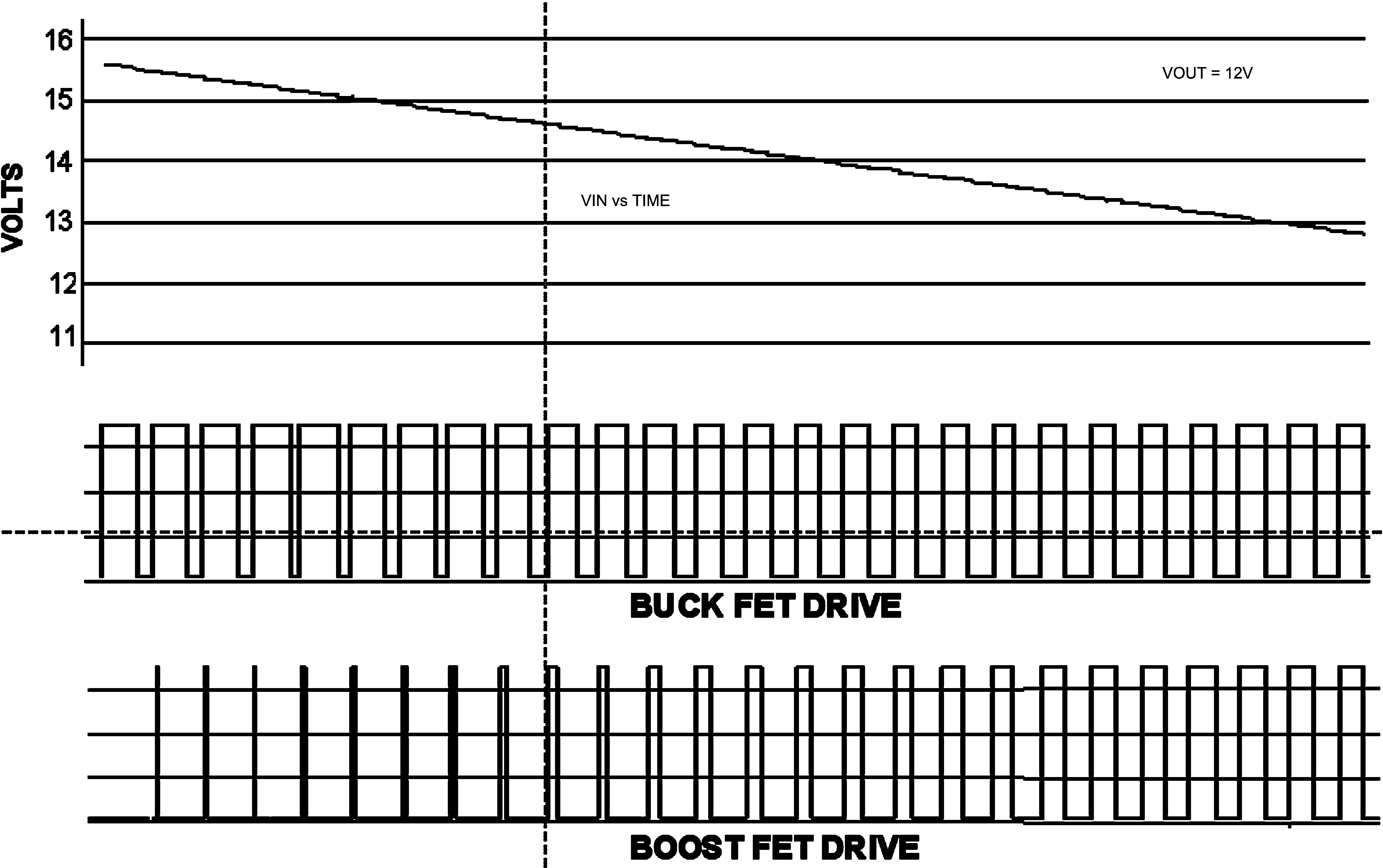
When VIN decreases relative to VOUT, the duty cycle of the buck switch will increase to maintain regulation. Once the duty cycle reaches 75%, the boost switch starts to operate with a very small duty cycle. As VIN is further decreased, the boost switch duty cycle increases until it is the same as the buck switch. As VIN is further decreased below VOUT, the buck and boost switch operate together with the same duty cycle and the regulator is in full buck-boost mode. This feature allows the regulator to transition smoothly from buck to buck-boost mode. Note that the regulator can be designed to operate with VIN less than 4 V, but VIN must be at least 5 V during start-up. Figure 16 shows a timing illustration of the gradual transition from buck to buck-boost mode when the input voltage ramps downward over a few switching cycles.
 Figure 16. Buck (HO) and Boost (LO) Switch Duty Cycle vs. Time,
Illustrating Gradual Mode Change With Decreasing Input Voltage