SNVS115E April   2000  – June 2019 LM2587

PRODUCTION DATA.  

  1. Features
  2. Typical Applications
  3. Description
    1.     Device Images
      1.      Flyback Regulator
  4. Revision History
  5. Pin Configurations
  6. Specifications
    1. 6.1  Absolute Maximum Ratings
    2. 6.2  ESDRatings
    3. 6.3  Recommended Operating Ratings
    4. 6.4  Thermal Information
    5. 6.5  Electrical Characteristics: 3.3 V
    6. 6.6  Electrical Characteristics: 5 V
    7. 6.7  Electrical Characteristics: 12 V
    8. 6.8  Electrical Characteristics: Adjustable
    9. 6.9  Electrical Characteristics: All Output Voltage Versions
    10. 6.10 Typical Characteristics
  7. Detailed Description
    1. 7.1 Overview
    2. 7.2 Functional Block Diagram
    3. 7.3 Feature Description
      1. 7.3.1 Step-Up (Boost) Regulator Operation
  8. Application And Implementation
    1. 8.1 Application Information
    2. 8.2 Typical Applications
      1. 8.2.1 Typical Boost Regulator Applications
      2. 8.2.2 Typical Flyback Regulator Applications
        1. 8.2.2.1 Transformer Selection (T)
        2. 8.2.2.2 Transformer Footprints
          1. 8.2.2.2.0.1 T4
      3. 8.2.3 Design Requirements
      4. 8.2.4 Detailed Design Procedure
        1. 8.2.4.1 Custom Design With Webench® Tools
        2. 8.2.4.2 Programming Output Voltage (Selecting R1 And R2)
        3. 8.2.4.3 Short Circuit Condition
        4. 8.2.4.4 Flyback Regulator Input Capacitors
        5. 8.2.4.5 Switch Voltage Limits
        6. 8.2.4.6 Output Voltage Limitations
        7. 8.2.4.7 Noisy Input Line Condition)
        8. 8.2.4.8 Stability
    3. 8.3 Additional Application Examples
      1. 8.3.1 Test Circuits
  9. Layout
    1. 9.1 Layout Guidelines
    2. 9.2 Layout Example
    3. 9.3 Heat Sink/Thermal Considerations
      1. 9.3.1 European Magnetic Vendor Contacts
      2. 9.3.2 Coilcraft
      3. 9.3.3 Pulse Engineering
  10. 10Device and Documentation Support
    1. 10.1 Device Support
      1. 10.1.1 Third-Party Products Disclaimer
      2. 10.1.2 Development Support
        1. 10.1.2.1 Custom Design With Webench® Tools
    2. 10.2 Receiving Notification Of Documentation Updates
    3. 10.3 Community Resources
    4. 10.4 Trademarks
    5. 10.5 Electrostatic Discharge Caution
    6. 10.6 Glossary
  11. 11Mechanical, Packaging, and Orderable Information

Package Options

Mechanical Data (Package|Pins)
Thermal pad, mechanical data (Package|Pins)
Orderable Information

Step-Up (Boost) Regulator Operation

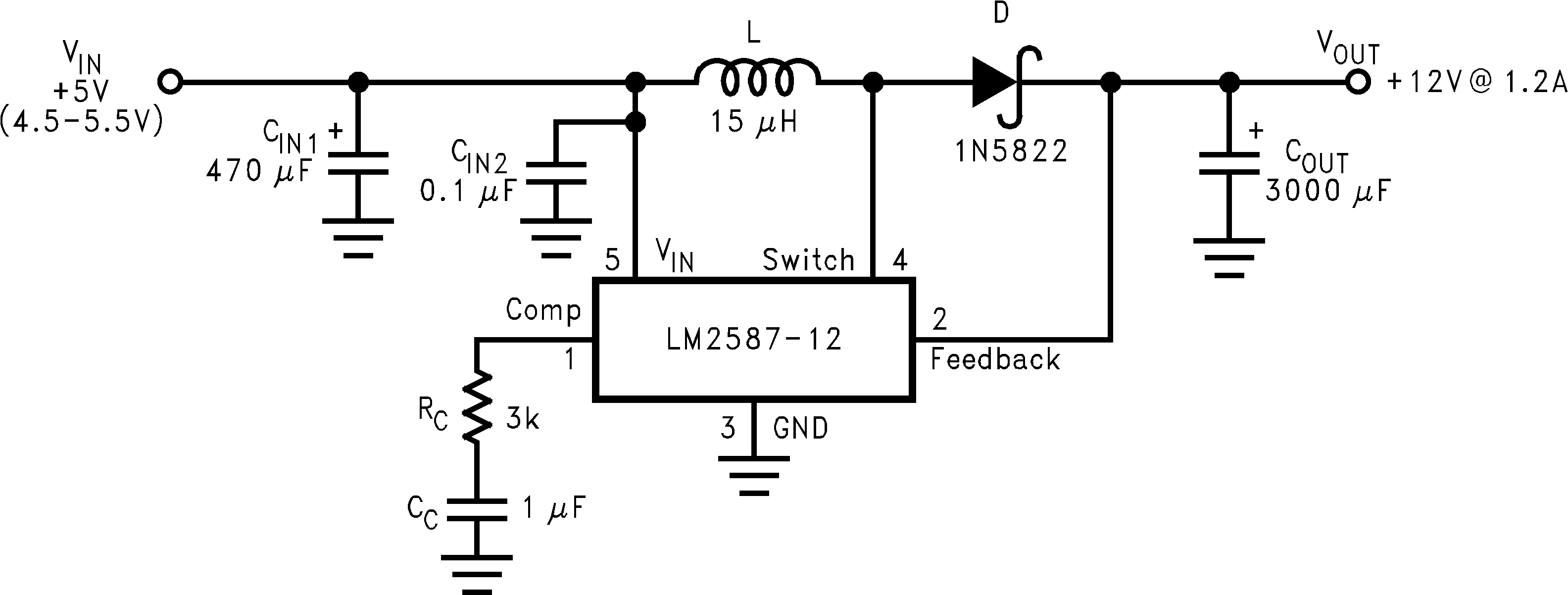
Figure 16 shows the LM2587 used as a step-up (boost) regulator. This is a switching regulator that produces an output voltage greater than the input supply voltage.

A brief explanation of how the LM2587 Boost Regulator works is as follows (refer to Figure 16). When the NPN switch turns on, the inductor current ramps up at the rate of VIN/L, storing energy in the inductor. When the switch turns off, the lower end of the inductor flies above VIN, discharging its current through diode (D) into the output capacitor (COUT) at a rate of (VOUT − VIN)/L. Thus, energy stored in the inductor during the switch on time is transferred to the output during the switch off time. The output voltage is controlled by adjusting the peak switch current, as described in the section.
LM2587 1231619.png
By adding a small number of external components (as shown in Figure 16), the LM2587 can be used to produce a regulated output voltage that is greater than the applied input voltage. The switching waveforms observed during the operation of this circuit are shown in . Typical performance of this regulator is shown in .
Figure 16. 12-V Boost Regulator