SNIS115S May 2001 – September 2015 LM26
PRODUCTION DATA.
- 1 Features
- 2 Applications
- 3 Description
- 4 Revision History
- 5 Device Comparison Table
- 6 Pin Configuration and Functions
- 7 Specifications
- 8 Detailed Description
- 9 Application and Implementation
- 10Power Supply Recommendations
- 11Layout
- 12Device and Documentation Support
- 13Mechanical, Packaging, and Orderable Information
Package Options
Mechanical Data (Package|Pins)
- DBV|5
Thermal pad, mechanical data (Package|Pins)
Orderable Information
8 Detailed Description
8.1 Overview
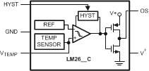
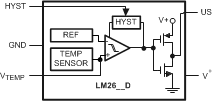
The LM26 is a factory preset thermostat (temperature switch) that includes an integrated temperature sensor, reference voltage, DAC and comparator. The LM26 can be factory programmed to have a trip point anywhere in the range of −55°C to +120°C. The output functionality can also be changed during the manufacturing process, as described in the functional block diagrams. Available options include:
- OS: active low, open drain that indicates an over temperature shutdown event (most common)
- US: active low, open-drain that indicates an under temperature shutdown event
- OS: active high, push-pull that indicates an over temperature shutdown event
- US: active high, push-pull that indicates an under temperature shutdown event
The internal temperature sensor is brought out on the VTEMP pin and can be used to determine the temperature that the LM26 is reading by monitoring with an ADC. It has a negative temperature coefficient (NTC) of approximately -10mV/°C. This pin also allows after assembly PCB testing (see section After Assembly PCB Testing for more details).
The comparator hysteresis is selectable by the state of the HYST. Two values are available 10°C or 2°C. Comparator hysteresis is essential, as it prevents comparator output chattering when the temperature is at the comparator threshold set point (REF as shown in the functional block diagrams). Once the comparator trips the hysteresis function changes the comparator threshold (REF) level such that the output remains locked in the active state. The threshold is changed by either 10°C or 2°C as programmed by the state of the HYST pin.
8.2 Functional Block Diagrams
 Figure 2. LM26-_ _A Output Pin Block Diagram
 Figure 3. LM26-_ _B Output Pin Block Diagram
 Figure 4. LM26-_ _C Output Pin Block Diagram
 Figure 5. LM26-_ _D Output Pin Block Diagram
8.3 Feature Description
8.3.1 Hysteresis
The HYST pin level sets the comparator hysteresis. Setting the HYST pin to GND selects 10°C hysteresis, while setting it to V+ selects 2°C. A series resistor can be used for protection purposes. The input leakage current of the pin is less than 10 µA. The value of the resistor will depend on the value of V+ as well as the leakage current. For example with V+ = 3.3 V the input threshold level for VIH = 0.8 × 3.3 V = 2.64 V, thus the voltage drop across the resistor should be less than 0.66 V. The 10-µA input leakage current requires the resistor value to be less than 66 kΩ.
8.3.2 VTEMP Output
The VTEMP output provides an output voltage that can be used to determine the temperature reading of the LM26. The temperature reading of the LM26 can be calculated using the equation:

or

The VTEMP output has very weak drive capability (1-µA source, 40-µA sink). So care should be taken when attaching circuitry to this pin. Capacitive loading may cause the VTEMP output to oscillate. Simply adding a resistor in series as shown in Figure 6 and Figure 7 will prevent oscillations from occurring. To determine the value of the resistor follow the guidelines given in Table 1. The same value resistor will work for either placement of the resistor. If an additional capacitive load is placed directly on the LM26 output, rather than across CLOAD, it should be at least a factor of 10 smaller than CLOAD.
Table 1. Resistive Compensation for Capacitive Loading of VTEMP
| CLOAD | R (Ω) |
|---|---|
| ≤100pF | 0 |
| 1nF | 8200 |
| 10nF | 3000 |
| 100nF | 1000 |
| ≥1µF | 430 |
 Figure 6. Resistor Placement for Capacitive-Loading Compensation of VTEMP With R in Series With Capacitor
 Figure 7. Resistor Placement for Capacitive-Loading Compensation of VTEMP With R in Series With Signal Path
8.4 Device Functional Modes
The LM26 after factory programming has two functional modes one with 2°C Hysteresis and the other with 10°C hysteresis as programmed by the level of the HYST pin. Selection of the level will depend on the system noise and the temperature transition rate.
8.4.1 After Assembly PCB Testing
The LM26's VTEMP output allows after-assembly PCB testing by following a simple test procedure. Simply measuring the VTEMP output voltage will verify that the LM26 has been assembled properly and that its temperature sensing circuitry is functional. The VTEMP output has very weak drive capability that can be overdriven by 1.5mA. Therefore, one can simply force the VTEMP voltage to cause the digital output to change state, thereby verifying that the comparator and output circuitry function after assembly. Here is a sample test procedure that can be used to test the LM26CIM5-TPA which has an 85°C trip point.
- Turn on V+ and measure VTEMP. Then calculate the temperature reading of the LM26 using the equation:
- Verify that the temperature measured in step one is within (±3°C + error of reference temperature sensor) of the ambient/board temperature. The ambient/board temperature (reference temperature) should be measured using an extremely accurate calibrated temperature sensor.
-
- Observe that OS is high.
- Drive VTEMP to ground.
- Observe that OS is now low.
- Release the VTEMP pin.
- Observe that OS is now high.
-
- Observe that OS is high.
- Drive VTEMP voltage down gradually.
- When OS goes low, note the VTEMP voltage.
- VTEMPTrig = VTEMP at OS trigger (HIGH->LOW)
- Calculate Trig using Equation 2.
-
- Gradually raise VTEMP until OS goes HIGH. Note VTEMP.
- Calculate THYST using Equation 2.

or
