SNVS136L September 1998 – June 2016 LM2672
PRODUCTION DATA.
- 1 Features
- 2 Applications
- 3 Description
- 4 Revision History
- 5 Description (continued)
- 6 Pin Configuration and Functions
-
7 Specifications
- 7.1 Absolute Maximum Ratings
- 7.2 ESD Ratings
- 7.3 Recommended Operating Conditions
- 7.4 Thermal Information
- 7.5 Electrical Characteristics - 3.3 V
- 7.6 Electrical Characteristics - 5 V
- 7.7 Electrical Characteristics - 12 V
- 7.8 Electrical Characteristics - Adjustable
- 7.9 Electrical Characteristics - All Output Voltage Versions
- 7.10 Typical Characteristics
- 7.11 Typical Characteristics - Fixed Output Voltage Versions
- 8 Parameter Measurement Information
- 9 Detailed Description
-
10Application and Implementation
- 10.1 Application Information
- 10.2
Typical Applications
- 10.2.1 Typical Application for Fixed Output Voltage Versions
- 10.2.2 Typical Application for Adjustable Output Voltage Versions
- 11Power Supply Recommendations
- 12Layout
- 13Device and Documentation Support
- 14Mechanical, Packaging, and Orderable Information
Package Options
Mechanical Data (Package|Pins)
Thermal pad, mechanical data (Package|Pins)
Orderable Information
7 Specifications
7.1 Absolute Maximum Ratings
over recommended operating junction temperature range of –40°C to 125°C (unless otherwise noted)(1)| MIN | MAX | UNIT | |||
|---|---|---|---|---|---|
| Supply voltage | 45 | V | |||
| ON/OFF pin voltage, VSH | –0.1 | 6 | V | ||
| Switch voltage to ground | –1 | V | |||
| Boost pin voltage | VSW + 8 | V | |||
| Feedback pin voltage, VFB | –0.3 | 14 | V | ||
| Power dissipation | Internally limited | ||||
| Lead temperature | D package | Vapor phase (60s) | 215 | °C | |
| Infrared (15s) | 220 | ||||
| P package (soldering, 10s) | 260 | ||||
| Maximum junction temperature, TJ | 150 | °C | |||
| Storage temperature, Tstg | –65 | 150 | °C | ||
(1) Stresses beyond those listed under Absolute Maximum Ratings may cause permanent damage to the device. These are stress ratings only, which do not imply functional operation of the device at these or any other conditions beyond those indicated under Recommended Operating Conditions. Exposure to absolute-maximum-rated conditions for extended periods may affect device reliability.
7.2 ESD Ratings
| VALUE | UNIT | |||
|---|---|---|---|---|
| V(ESD) | Electrostatic discharge | Human-body model (HBM), per ANSI/ESDA/JEDEC JS-001(1) | ±2000 | V |
(1) JEDEC document JEP155 states that 500-V HBM allows safe manufacturing with a standard ESD control process.
7.3 Recommended Operating Conditions
over operating free-air temperature range (unless otherwise noted)| MIN | MAX | UNIT | ||
|---|---|---|---|---|
| Supply voltage | 6.5 | 40 | V | |
| TJ | Operating junction temperature | –40 | 125 | °C |
7.4 Thermal Information
| THERMAL METRIC(1)(2) | LM2672 | UNIT | |||
|---|---|---|---|---|---|
| D (SOIC) | P (PDIP) | WSON (NHN) | |||
| 8 PINS | 8 PINS | 16 PINS | |||
| RθJA | Junction-to-ambient thermal resistance | 105 | 95 | — | °C/W |
| RθJC(top) | Junction-to-case (top) thermal resistance | — | — | — | °C/W |
| RθJB | Junction-to-board thermal resistance | — | — | — | °C/W |
| ψJT | Junction-to-top characterization parameter | — | — | — | °C/W |
| ψJB | Junction-to-board characterization parameter | — | — | — | °C/W |
| RθJC(bot) | Junction-to-case (bottom) thermal resistance | — | — | — | °C/W |
(1) For more information about traditional and new thermal metrics, see the Semiconductor and IC Package Thermal Metrics application report.
(2) Thermal resistances were simulated on 4-layer JEDEC board.
7.5 Electrical Characteristics – 3.3 V
TJ = 25°C (unless otherwise noted; see Figure 19)(1)| PARAMETER | TEST CONDITIONS | MIN(2) | TYP(3) | MAX(2) | UNIT | ||
|---|---|---|---|---|---|---|---|
| VOUT | Output voltage | VIN = 8 V to 40 V, ILOAD = 20 mA to 1 A | TJ = 25°C | 3.251 | 3.3 | 3.35 | V |
| TJ = –40°C to 125°C | 3.201 | 3.399 | |||||
| VIN = 6.5 V to 40 V, ILOAD = 20 mA to 500 mA |
TJ = 25°C | 3.35 | 3.3 | 3.35 | |||
| TJ = –40°C to 125°C | 3.201 | 3.399 | |||||
| η | Efficiency | VIN = 12 V, ILOAD = 1 A | 86% | ||||
(1) External components such as the catch diode, inductor, input and output capacitors, and voltage programming resistors can affect switching regulator performance. When the LM2672 is used as shown in Figure 19 test circuits, system performance is as specified by the system parameters section of Electrical Characteristics.
(2) All limits specified at room temperature and at temperature extremes. All room temperature limits are 100% production tested. All limits at temperature extremes are specified through correlation using standard Statistical Quality Control (SQC) methods. All limits are used to calculate Average Outgoing Quality Level (AOQL).
(3) Typical numbers are at 25°C and represent the most likely norm.
7.6 Electrical Characteristics – 5 V
TJ = 25°C (unless otherwise noted; see Figure 19)(1)| PARAMETER | TEST CONDITIONS | MIN(2) | TYP(3) | MAX(2) | UNIT | ||
|---|---|---|---|---|---|---|---|
| VOUT | Output voltage | VIN = 8 V to 40 V, ILOAD = 20 mA to 1 A | TJ = 25°C | 4.925 | 5 | 5.075 | V |
| TJ = –40°C to 125°C | 4.85 | 5.15 | |||||
| VIN = 6.5 V to 40 V, ILOAD = 20 mA to 500 mA |
TJ = 25°C | 4.925 | 5 | 5.075 | |||
| TJ = –40°C to 125°C | 4.85 | 5.15 | |||||
| η | Efficiency | VIN = 12 V, ILOAD = 1 A | 90% | ||||
(1) External components such as the catch diode, inductor, input and output capacitors, and voltage programming resistors can affect switching regulator performance. When the LM2672 is used as shown in Figure 19 test circuits, system performance is as specified by the system parameters section of Electrical Characteristics.
(2) All limits specified at room temperature and at temperature extremes. All room temperature limits are 100% production tested. All limits at temperature extremes are specified through correlation using standard Statistical Quality Control (SQC) methods. All limits are used to calculate Average Outgoing Quality Level (AOQL).
(3) Typical numbers are at 25°C and represent the most likely norm.
7.7 Electrical Characteristics – 12 V
TJ = 25°C (unless otherwise noted; see Figure 19)(1)| PARAMETER | TEST CONDITIONS | MIN(2) | TYP(3) | MAX(2) | UNIT | ||
|---|---|---|---|---|---|---|---|
| VOUT | Output voltage | VIN = 15 V to 40 V, ILOAD = 20 mA to 1 A | TJ = 25°C | 11.82 | 12 | 12.18 | V |
| TJ = –40°C to 125°C | 11.64 | 12.36 | |||||
| η | Efficiency | VIN = 24 V, ILOAD = 1 A | 94% | ||||
(1) External components such as the catch diode, inductor, input and output capacitors, and voltage programming resistors can affect switching regulator performance. When the LM2672 is used as shown in Figure 19 test circuits, system performance is as specified by the system parameters section of Electrical Characteristics.
(2) All limits specified at room temperature and at temperature extremes. All room temperature limits are 100% production tested. All limits at temperature extremes are specified through correlation using standard Statistical Quality Control (SQC) methods. All limits are used to calculate Average Outgoing Quality Level (AOQL).
(3) Typical numbers are at 25°C and represent the most likely norm.
7.8 Electrical Characteristics – Adjustable
TJ = 25°C (unless otherwise noted; see Figure 19)(1)| PARAMETER | TEST CONDITIONS | MIN(2) | TYP(3) | MAX(2) | UNIT | ||
|---|---|---|---|---|---|---|---|
| VFB | Feedback voltage | VIN = 8 V to 40 V, ILOAD = 20 mA to 1 A, VOUT programmed for 5 V (see Figure 19) | TJ = 25°C | 1.192 | 1.21 | 1.228 | V |
| TJ = –40°C to 125°C | 1.174 | 1.246 | |||||
| VIN = 6.5 V to 40 V, ILOAD = 20 mA to 500 mA, VOUT programmed for 5 V (see Figure 19) | TJ = 25°C | 1.192 | 1.21 | 1.228 | |||
| TJ = –40°C to 125°C | 1.174 | 1.246 | |||||
| η | Efficiency | VIN = 12 V, ILOAD = 1 A | 90% | ||||
(1) External components such as the catch diode, inductor, input and output capacitors, and voltage programming resistors can affect switching regulator performance. When the LM2672 is used as shown in Figure 19 test circuits, system performance is as specified by the system parameters section of Electrical Characteristics.
(2) All limits specified at room temperature and at temperature extremes. All room temperature limits are 100% production tested. All limits at temperature extremes are specified through correlation using standard Statistical Quality Control (SQC) methods. All limits are used to calculate Average Outgoing Quality Level (AOQL).
(3) Typical numbers are at 25°C and represent the most likely norm.
7.9 Electrical Characteristics – All Output Voltage Versions
TJ = 25°C, VIN = 12 V for the 3.3 V, 5 V, and Adjustable versions and VIN = 24V for the 12V version, and ILOAD = 100 mA (unless otherwise noted)| PARAMETER | TEST CONDITIONS | MIN(1) | TYP(2) | MAX(1) | UNIT | ||
|---|---|---|---|---|---|---|---|
| IQ | Quiescent current | VFEEDBACK = 8 V for 3.3 V, 5 V, and adjustable versions | 2.5 | 3.6 | mA | ||
| VFEEDBACK = 15 V for 12 V versions | 2.5 | ||||||
| ISTBY | Standby quiescent current | ON/OFF Pin = 0 V | TJ = 25°C | 50 | 100 | μA | |
| TJ = –40°C to 125°C | 150 | ||||||
| ICL | Current limit | 1.25 | 1.55 | 2.1 | A | ||
| 1.2 | 2.2 | ||||||
| IL | Output leakage current | VSWITCH = 0 V, ON/OFF Pin = 0 V, VIN = 40 V | 1 | 25 | μA | ||
| VSWITCH = −1 V, ON/OFF Pin = 0 V | 6 | 15 | mA | ||||
| RDS(ON) | Switch on-resistance | ISWITCH = 1 A | TJ = 25°C | 0.25 | 0.3 | Ω | |
| TJ = –40°C to 125°C | 0.5 | ||||||
| fO | Oscillator frequency | Measured at switch pin | TJ = 25°C | 260 | kHz | ||
| TJ = –40°C to 125°C | 225 | 275 | |||||
| D | Maximum duty cycle | TJ = 25°C | 95% | ||||
| Minimum duty cycle | TJ = –40°C to 125°C | 0% | |||||
| IBIAS | Feedback bias current | VFEEDBACK = 1.3 V, adjustable version only | 85 | nA | |||
| VS/D | ON/OFF pin voltage | TJ = 25°C | 1.4 | V | |||
| TJ = –40°C to 125°C | 0.8 | 2 | |||||
| IS/D | ON/OFF pin current | ON/OFF Pin = 0 V | TJ = 25°C | 20 | μA | ||
| TJ = –40°C to 125°C | 7 | 37 | |||||
| FSYNC | Synchronization frequency | VSYNC = 3.5 V, 50% duty cycle | 400 | kHz | |||
| VSYNC | Synchronization threshold voltage | 1.4 | V | ||||
| VSS | Soft-start voltage | TJ = 25°C | 0.63 | V | |||
| TJ = –40°C to 125°C | 0.53 | 0.73 | |||||
| ISS | Soft-start current | TJ = 25°C | 4.5 | μA | |||
| TJ = –40°C to 125°C | 1.5 | 6.9 | |||||
(1) All limits specified at room temperature and at temperature extremes. All room temperature limits are 100% production tested. All limits at temperature extremes are specified through correlation using standard Statistical Quality Control (SQC) methods. All limits are used to calculate Average Outgoing Quality Level (AOQL).
(2) Typical numbers are at 25°C and represent the most likely norm.
7.10 Typical Characteristics
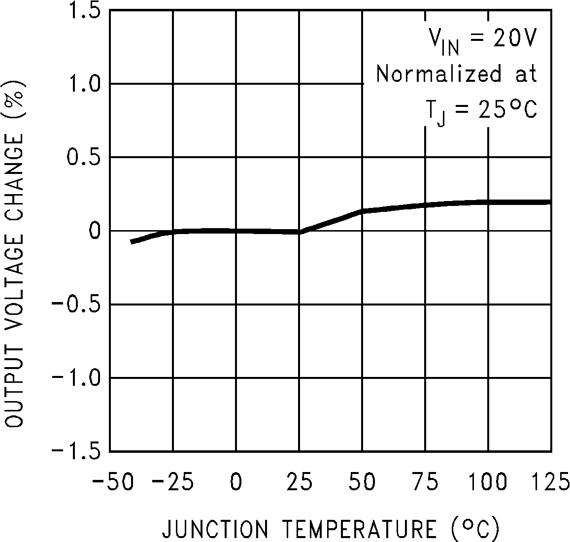 Figure 1. Normalized Output Voltage
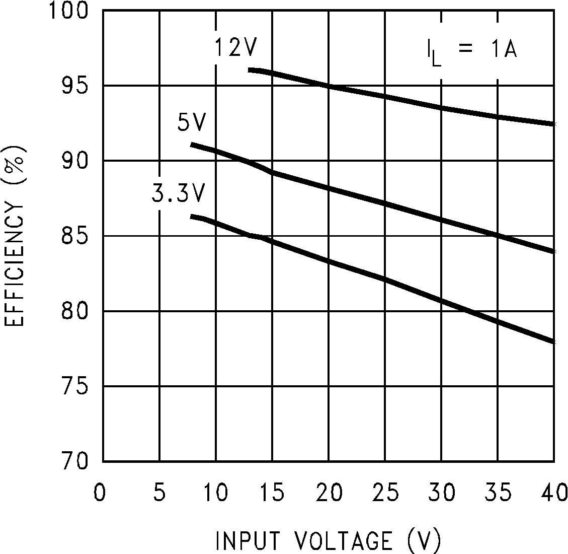 Figure 3. Efficiency
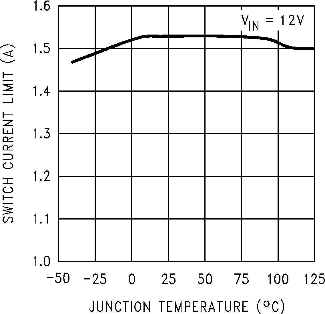 Figure 5. Switch Current Limit
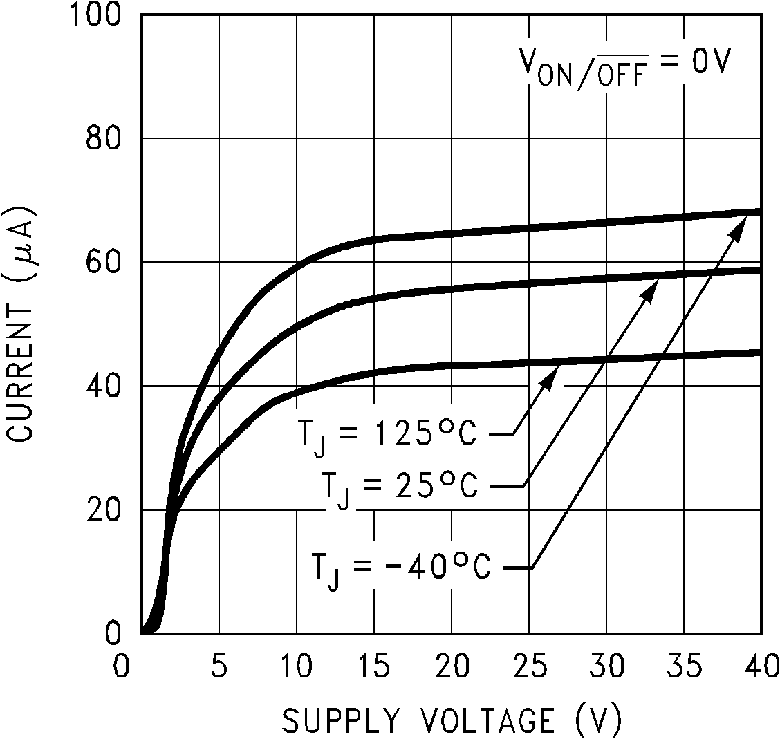 Figure 7. Standby Quiescent Current
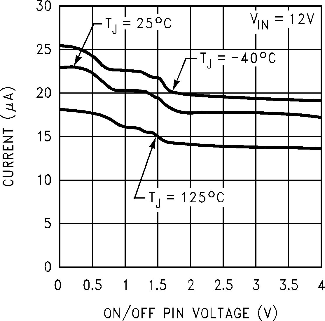 Figure 9. ON/OFF Pin Current (Sourcing)
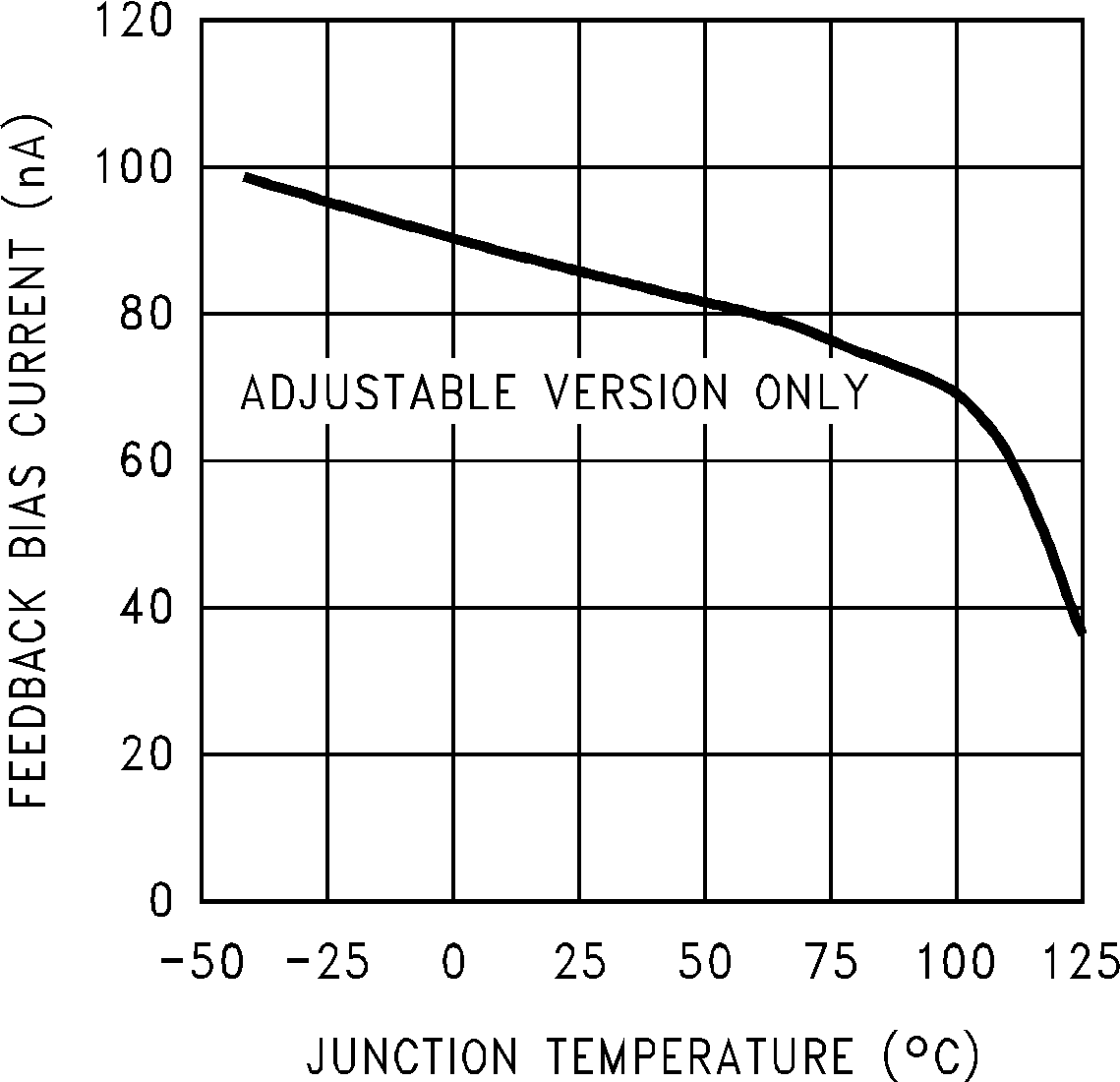 Figure 11. Feedback Pin Bias Current
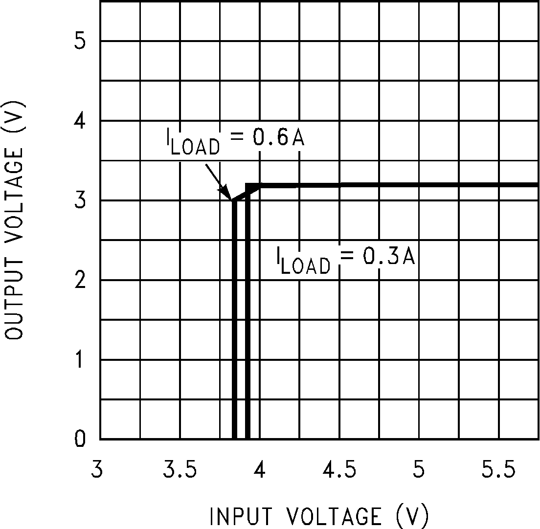 Figure 13. Dropout Voltage, 3.3-V Option
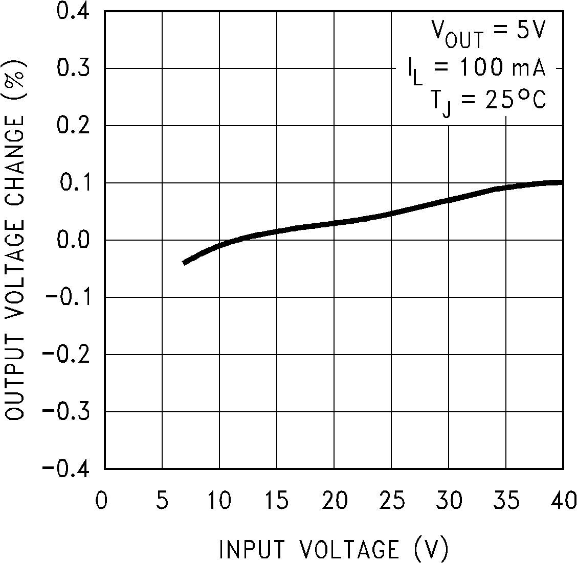 Figure 2. Line Regulation
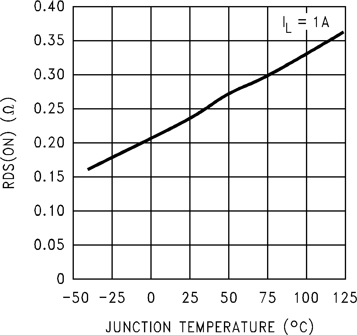 Figure 4. Drain-to-Source Resistance
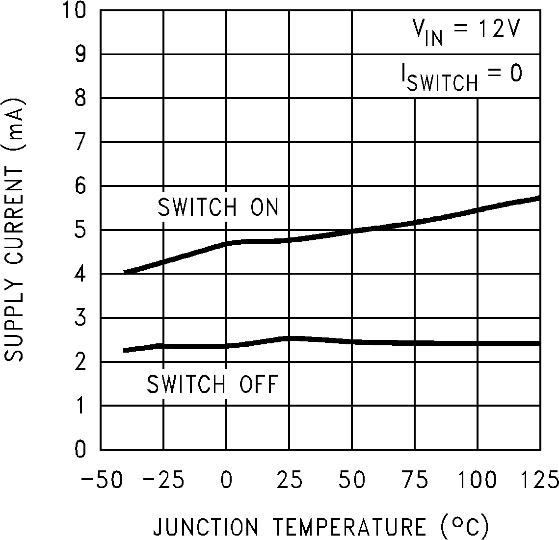 Figure 6. Operating Quiescent Current
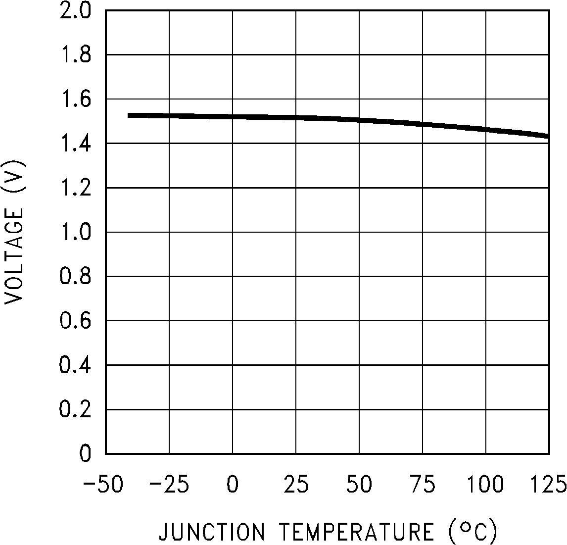 Figure 8. ON/OFF Threshold Voltage
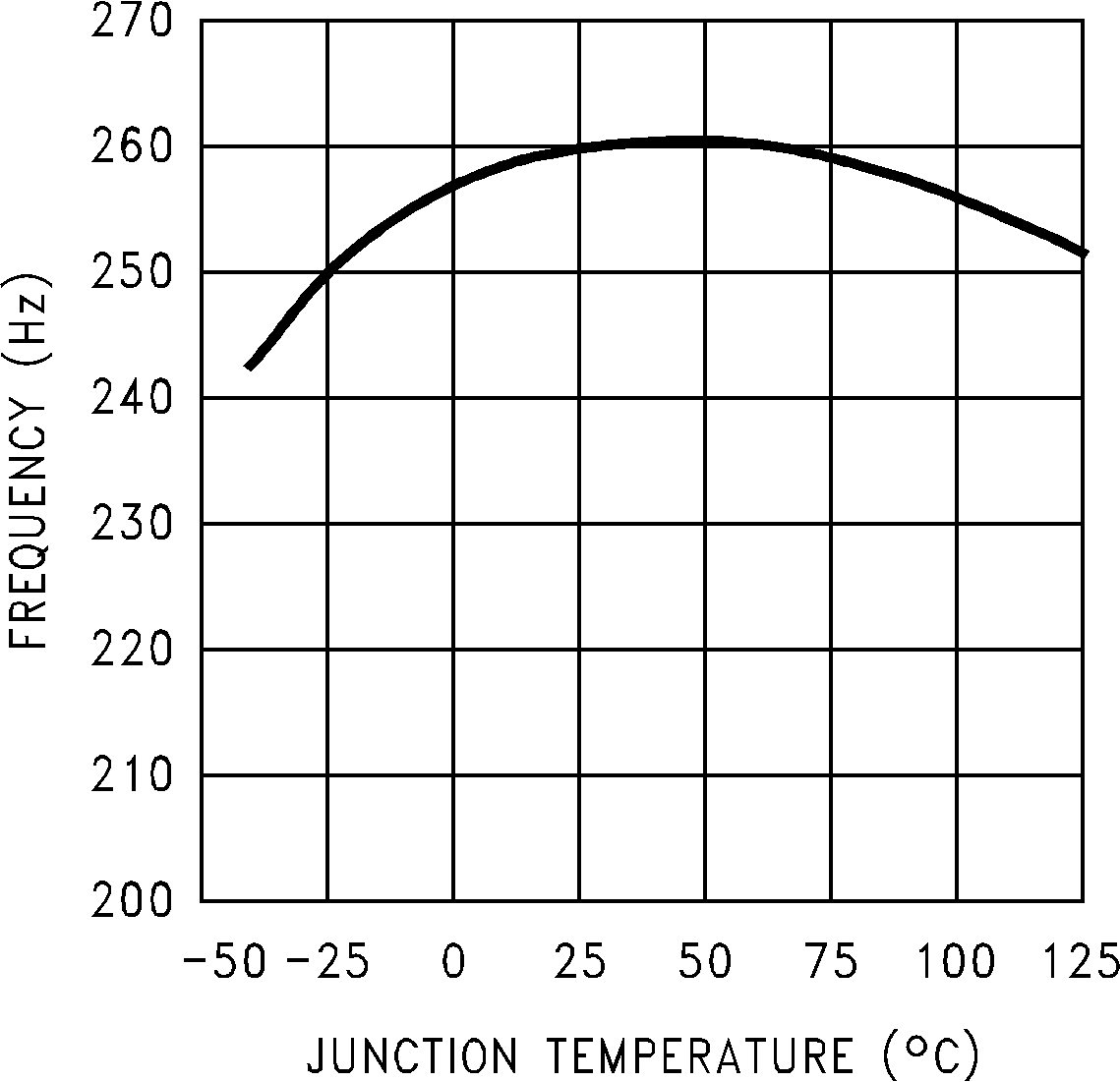 Figure 10. Switching Frequency
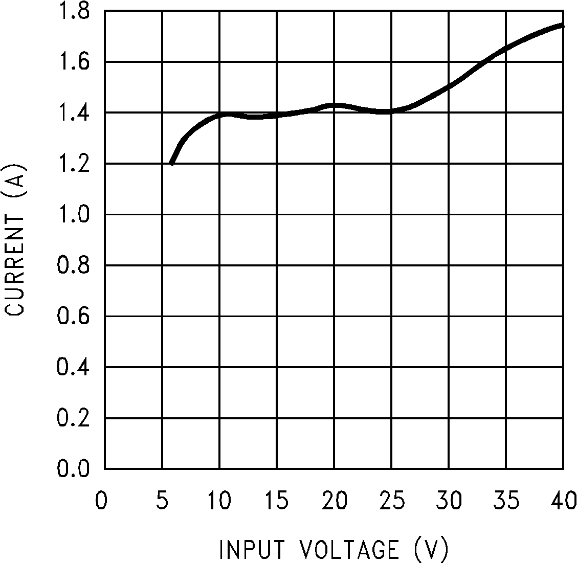 Figure 12. Peak Switch Current
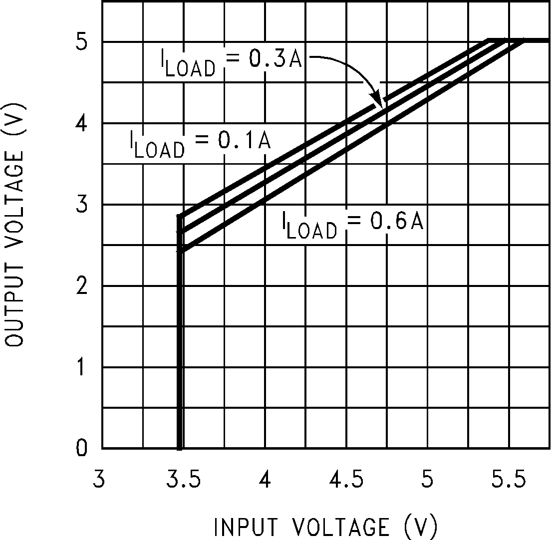 Figure 14. Dropout Voltage, 5-V Option
7.11 Typical Characteristics – Fixed Output Voltage Versions
see Figure 19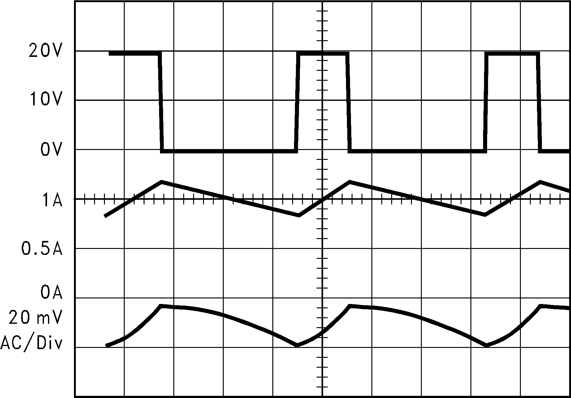
| VSW pin voltage, 10 V/div | VIN = 20 V, VOUT = 5 V, |
| Inductor current, 0.5 A/div | ILOAD = 1 A, L = 47 μH, |
| Output ripple voltage, 20 mV/div AC-coupled |
COUT = 68 μF, COUTESR = 50 mΩ |
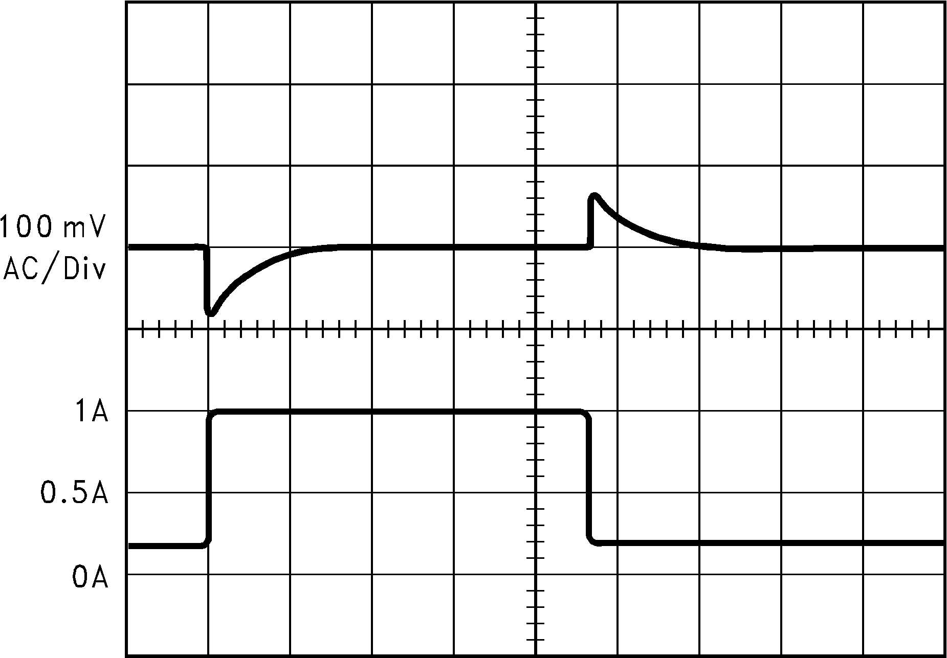
| Output voltage, | VIN = 20 V, VOUT = 5 V, |
| 100 mV/div, AC-coupled | ILOAD = 1 A, L = 47 μH, |
| Load current: 200 mA to 1 A load pulse |
COUT = 68 μF, COUTESR = 50 mΩ |
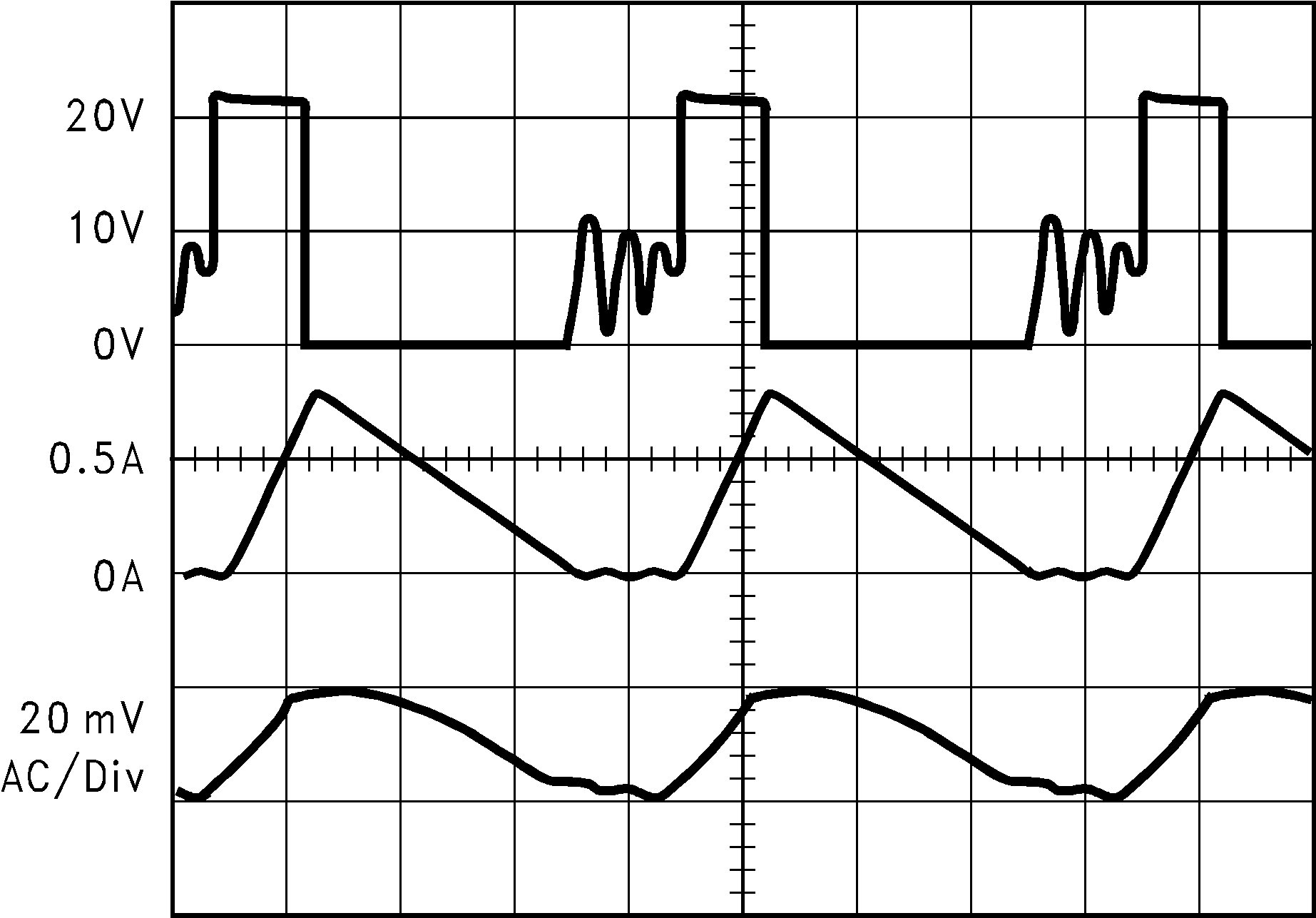
| VSW pin voltage, 10 V/div | VIN = 20 V, VOUT = 5 V, |
| Inductor current, 0.5 A/div | ILOAD = 300 mA, L = 15 μH, |
| Output ripple voltage, 20 mV/div AC-coupled |
COUT = 68 μF (2×), COUTESR = 25 mΩ |
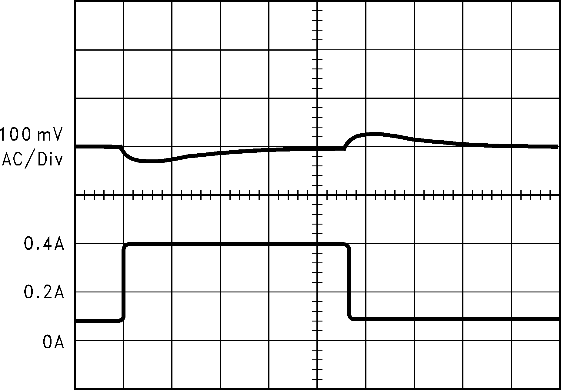
| Output voltage, | VIN = 20 V, VOUT = 5 V, |
| 100 mV/div, AC-coupled | L = 47 μH, |
| Load current: 100 mA to 300 mA load pulse |
COUT = 68 μF, COUTESR = 50 mΩ |