SNVS026O March 2000 – June 2016 LM2679
PRODUCTION DATA.
- 1 Features
- 2 Applications
- 3 Description
- 4 Revision History
- 5 Pin Configuration and Functions
-
6 Specification
- 6.1 Absolute Maximum Ratings
- 6.2 ESD Ratings
- 6.3 Recommended Operating Conditions
- 6.4 Thermal Information
- 6.5 Electrical Characteristics - 3.3 V
- 6.6 Electrical Characteristics - 5 V
- 6.7 Electrical Characteristics - 12 V
- 6.8 Electrical Characteristics - Adjustable
- 6.9 Electrical Characteristics - All Output Voltage Versions
- 6.10 Typical Characteristics
- 7 Detailed Description
- 8 Application and Implementation
- 9 Power Supply Recommendations
- 10Layout
- 11Device and Documentation Support
- 12Mechanical, Packaging, and Orderable Information
Package Options
Mechanical Data (Package|Pins)
Thermal pad, mechanical data (Package|Pins)
- KTW|7
Orderable Information
6 Specification
6.1 Absolute Maximum Ratings
over operating free-air temperature range (unless otherwise noted)(1)(2)| MIN | MAX | UNIT | ||
|---|---|---|---|---|
| Input supply voltage | 45 | V | ||
| Soft-start pin voltage | –0.1 | 6 | V | |
| Switch voltage to ground(3) | –1 | VIN | V | |
| Boost pin voltage | VSW + 8 V | V | ||
| Feedback pin voltage | –0.3 | 14 | V | |
| Power dissipation | Internally limited | |||
| Soldering temperature | Wave (4 s) | 260 | °C | |
| Infrared (10 s) | 240 | |||
| Vapor phase (75 s) | 219 | |||
| Storage Temperature, Tstg | –65 | 150 | °C | |
(1) Stresses beyond those listed under Absolute Maximum Ratings may cause permanent damage to the device. These are stress ratings only, which do not imply functional operation of the device at these or any other conditions beyond those indicated under Recommended Operating Conditions. Exposure to absolute-maximum-rated conditions for extended periods may affect device reliability.
(2) If Military/Aerospace specified devices are required, please contact the Texas Instruments Sales Office/Distributors for availability and specifications.
(3) The absolute maximum specification of the switch voltage to ground applies to DC voltage. An extended negative voltage limit of –10 V applies to a pulse of up to 20 ns, –6 V of 60 ns and –3 V of up to 100 ns.
6.2 ESD Ratings
| VALUE | UNIT | |||
|---|---|---|---|---|
| V(ESD) | Electrostatic discharge | Human-body model (HBM), per ANSI/ESDA/JEDEC JS-001(1)(2) | ±2000 | V |
(1) JEDEC document JEP155 states that 500-V HBM allows safe manufacturing with a standard ESD control process.
(2) ESD was applied using the human-body model, a 100-pF capacitor discharged through a 1.5-kΩ resistor into each pin.
6.3 Recommended Operating Conditions
| MIN | MAX | UNIT | |
|---|---|---|---|
| Supply voltage | 8 | 40 | V |
| Junction temperature, TJ | –40 | 125 | °C |
6.4 Thermal Information
| THERMAL METRIC(1) | LM2679 | UNIT | ||||
|---|---|---|---|---|---|---|
| NDZ (TO-220) |
KTW (TO-263) |
NHM (VSON) |
||||
| 7 PINS | 7 PINS | 14 PINS | ||||
| RθJA | Junction-to-ambient thermal resistance | See(2) | 65 | — | — | °C/W |
| See(3) | 45 | — | — | |||
| See(4) | — | 56 | — | |||
| See(5) | — | 35 | — | |||
| See(6) | — | 26 | — | |||
| See(7) | — | — | 55 | |||
| See(8) | — | — | 29 | |||
| RθJC(top) | Junction-to-case (top) thermal resistance | 2 | 2 | — | °C/W | |
(1) For more information about traditional and new thermal metrics, see the Semiconductor and IC Package Thermal Metrics application report.
(2) Junction to ambient thermal resistance (no external heat sink) for the 7-lead TO-220 package mounted vertically, with ½ inch leads in a socket, or on a PCB with minimum copper area.
(3) Junction to ambient thermal resistance (no external heat sink) for the 7-lead TO-220 package mounted vertically, with ½ inch leads soldered to a PCB containing approximately 4 square inches of (1 oz.) copper area surrounding the leads.
(4) Junction to ambient thermal resistance for the 7-lead DDPAK mounted horizontally against a PCB area of 0.136 square inches (the same size as the DDPAK package) of 1 oz. (0.0014 in. thick) copper.
(5) Junction to ambient thermal resistance for the 7-lead DDPAK mounted horizontally against a PCB area of 0.4896 square inches
(3.6 times the area of the DDPAK package) of 1 oz. (0.0014 in. thick) copper.
(3.6 times the area of the DDPAK package) of 1 oz. (0.0014 in. thick) copper.
(6) Junction to ambient thermal resistance for the 7-lead DDPAK mounted horizontally against a PCB copper area of 1.0064 square inches (7.4 times the area of the DDPAK 3 package) of 1 oz. (0.0014 in. thick) copper. Additional copper area reduces thermal resistance further.
(7) Junction to ambient thermal resistance for the 14-lead VSON mounted on a PCB copper area equal to the die attach paddle.
(8) Junction to ambient thermal resistance for the 14-lead VSON mounted on a PCB copper area using 12 vias to a second layer of copper equal to die attach paddle. Additional copper area reduces thermal resistance further. For layout recommendations, see AN-1187 Leadless Leadfram Package (LLP).
6.5 Electrical Characteristics – 3.3 V
Specifications apply for TA = TJ = 25°C and RADJ = 5.6 kΩ (unless otherwise noted).| PARAMETER | TEST CONDITIONS | MIN(1) | TYP(2) | MAX(1) | UNIT | ||
|---|---|---|---|---|---|---|---|
| VOUT | Output voltage | VIN = 8 V to 40 V, 100 mA ≤ IOUT ≤ 5 A |
TJ = 25°C | 3.234 | 3.3 | 3.366 | V |
| TJ = –40°C to 125°C | 3.201 | 3.399 | |||||
| η | Efficiency | VIN = 12 V, ILOAD = 5 A | 82% | ||||
(1) All room temperature limits are 100% tested during production with TA = TJ = 25°C. All limits at temperature extremes are specified through correlation using standard Quality Control (SQC) methods. All limits are used to calculate Average Outgoing Quality Level (AOQL).
(2) Typical values are determined with TA = TJ = 25°C and represent the most likely norm.
6.6 Electrical Characteristics – 5 V
Specifications apply for TA = TJ = 25°C and RADJ = 5.6 kΩ (unless otherwise noted).| PARAMETER | TEST CONDITIONS | MIN(1) | TYP(2) | MAX(1) | UNIT | ||
|---|---|---|---|---|---|---|---|
| VOUT | Output voltage | VIN = 8 V to 40 V, 100 mA ≤ IOUT ≤ 5 A |
TJ = 25°C | 4.9 | 5 | 5.1 | V |
| TJ = –40°C to 125°C | 4.85 | 5.15 | |||||
| η | Efficiency | VIN = 12 V, ILOAD = 5 A | 84% | ||||
(1) All room temperature limits are 100% tested during production with TA = TJ = 25°C. All limits at temperature extremes are specified through correlation using standard Quality Control (SQC) methods. All limits are used to calculate Average Outgoing Quality Level (AOQL).
(2) Typical values are determined with TA = TJ = 25°C and represent the most likely norm.
6.7 Electrical Characteristics – 12 V
Specifications apply for TA = TJ = 25°C and RADJ = 5.6 kΩ (unless otherwise noted).| PARAMETER | TEST CONDITIONS | MIN(1) | TYP(2) | MAX(1) | UNIT | ||
|---|---|---|---|---|---|---|---|
| VOUT | Output voltage | VIN = 15 V to 40 V, 100 mA ≤ IOUT ≤ 5 A |
TJ = 25°C | 11.76 | 12 | 12.24 | V |
| TJ = –40°C to 125°C | 11.64 | 12.36 | |||||
| η | Efficiency | VIN = 24 V, ILOAD = 5 A | 92% | ||||
(1) All room temperature limits are 100% tested during production with TA = TJ = 25°C. All limits at temperature extremes are specified through correlation using standard Quality Control (SQC) methods. All limits are used to calculate Average Outgoing Quality Level (AOQL).
(2) Typical values are determined with TA = TJ = 25°C and represent the most likely norm.
6.8 Electrical Characteristics – Adjustable
Specifications apply for TA = TJ = 25°C and RADJ = 5.6 kΩ (unless otherwise noted).| PARAMETER | TEST CONDITIONS | MIN(1) | TYP(2) | MAX(1) | UNIT | ||
|---|---|---|---|---|---|---|---|
| VFB | Feedback voltage | VIN = 8 V to 40 V, 100 mA ≤ IOUT ≤ 5 A, VOUT programmed for 5 V |
TJ = 25°C | 1.186 | 1.21 | 1.234 | V |
| TJ = –40°C to 125°C | 1.174 | 1.246 | |||||
| η | Efficiency | VIN = 12 V, ILOAD = 5 A | 84% | ||||
(1) All room temperature limits are 100% tested during production with TA = TJ = 25°C. All limits at temperature extremes are specified through correlation using standard Quality Control (SQC) methods. All limits are used to calculate Average Outgoing Quality Level (AOQL).
(2) Typical values are determined with TA = TJ = 25°C and represent the most likely norm.
6.9 Electrical Characteristics – All Output Voltage Versions
Specifications are for TA = TJ = 25°C, VIN = 12 V for the 3.3 V, 5-V, and adjustable versions, and VIN = 24 V for the 12-V version (unless otherwise specified).| PARAMETER | TEST CONDITIONS | MIN | TYP | MAX | UNIT | ||
|---|---|---|---|---|---|---|---|
| IQ | Quiescent current | VFEEDBACK = 8 V for 3.3-V, 5-V, and adjustable versions, VFEEDBACK = 15 V for 12-V version |
4.2 | 6 | mA | ||
| VADJ | Current limit adjust voltage | TJ = 25°C | 1.181 | 1.21 | 1.229 | V | |
| TJ = –40°C to 125°C | 1.169 | 1.246 | |||||
| ICL | Current limit | RADJ = 5.6 kΩ(1) | TJ = 25°C | 5.5 | 6.3 | 7.6 | A |
| TJ = –40°C to 125°C | 5.3 | 8.1 | |||||
| IL | Output leakage current | VIN = 40 V, soft-start pin = 0 V | VSWITCH = 0 V | 1 | 1.5 | mA | |
| VSWITCH = −1 V | 6 | 15 | |||||
| RDS(ON) | Switch ON-resistance | ISWITCH = 5 A | TJ = 25°C | 0.12 | 0.14 | Ω | |
| TJ = –40°C to 125°C | 0.225 | ||||||
| fO | Oscillator frequency | Measured at switch pin | TJ = 25°C | 260 | kHz | ||
| TJ = –40°C to 125°C | 225 | 280 | |||||
| D | Duty cycle | Maximum duty cycle | 91% | ||||
| Minimum duty cycle | 0% | ||||||
| IBIAS | Feedback bias current |
VFEEDBACK = 1.3 V (adjustable version only) | 85 | nA | |||
| VSFST | Soft-start threshold voltage | TJ = 25°C | 0.63 | V | |||
| TJ = –40°C to 125°C | 0.53 | 0.74 | |||||
| ISFST | Soft-start pin current | Soft-start pin = 0 V | TJ = 25°C | 3.7 | μA | ||
| TJ = –40°C to 125°C | 6.9 | ||||||
(1) The peak switch current limit is determined by the following relationship: ICL = 37,125 / RADJ
6.10 Typical Characteristics
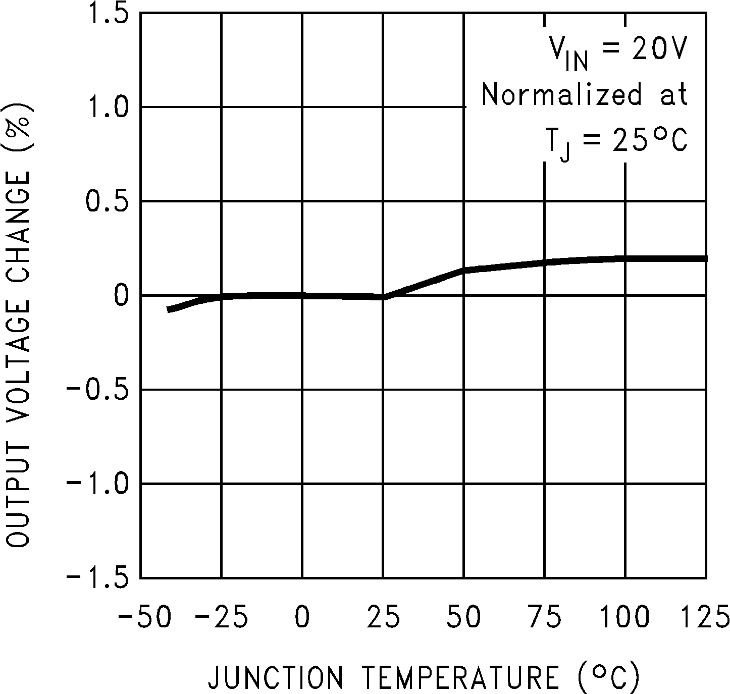 Figure 1. Normalized Output Voltage
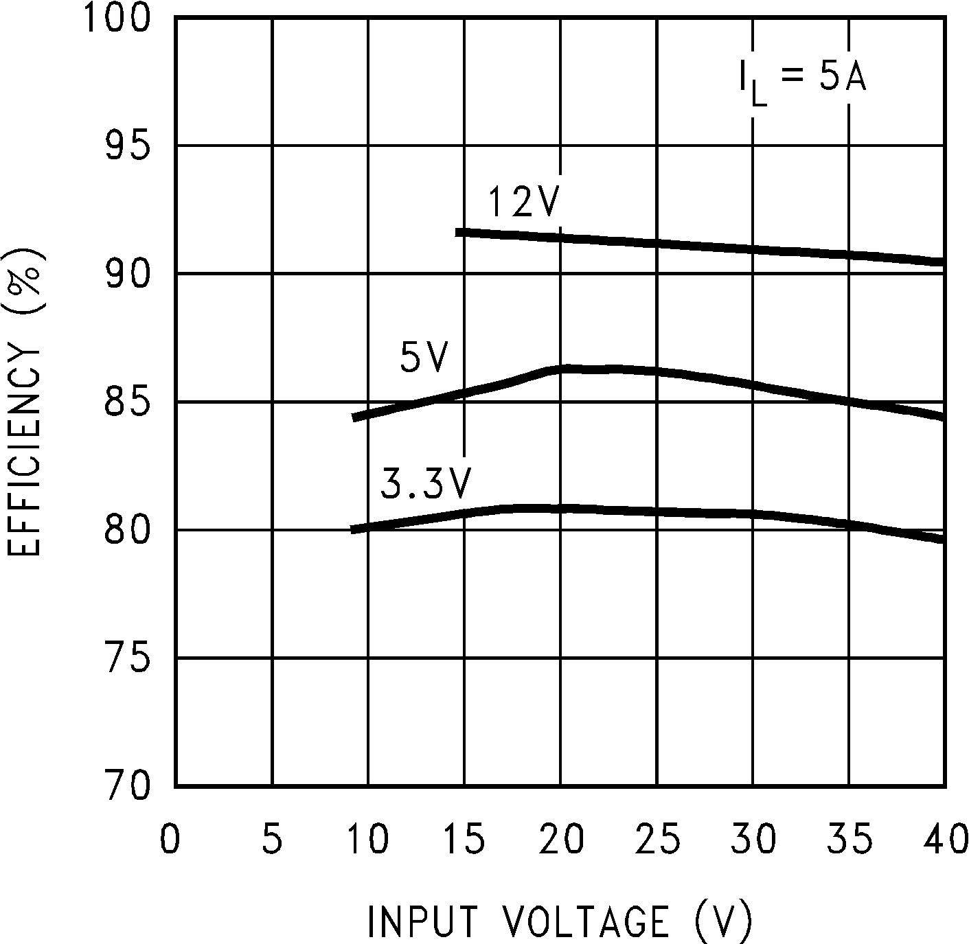 Figure 3. Efficiency vs Input Voltage
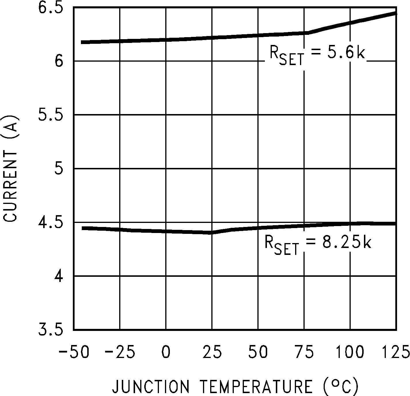 Figure 5. Switch Current Limit
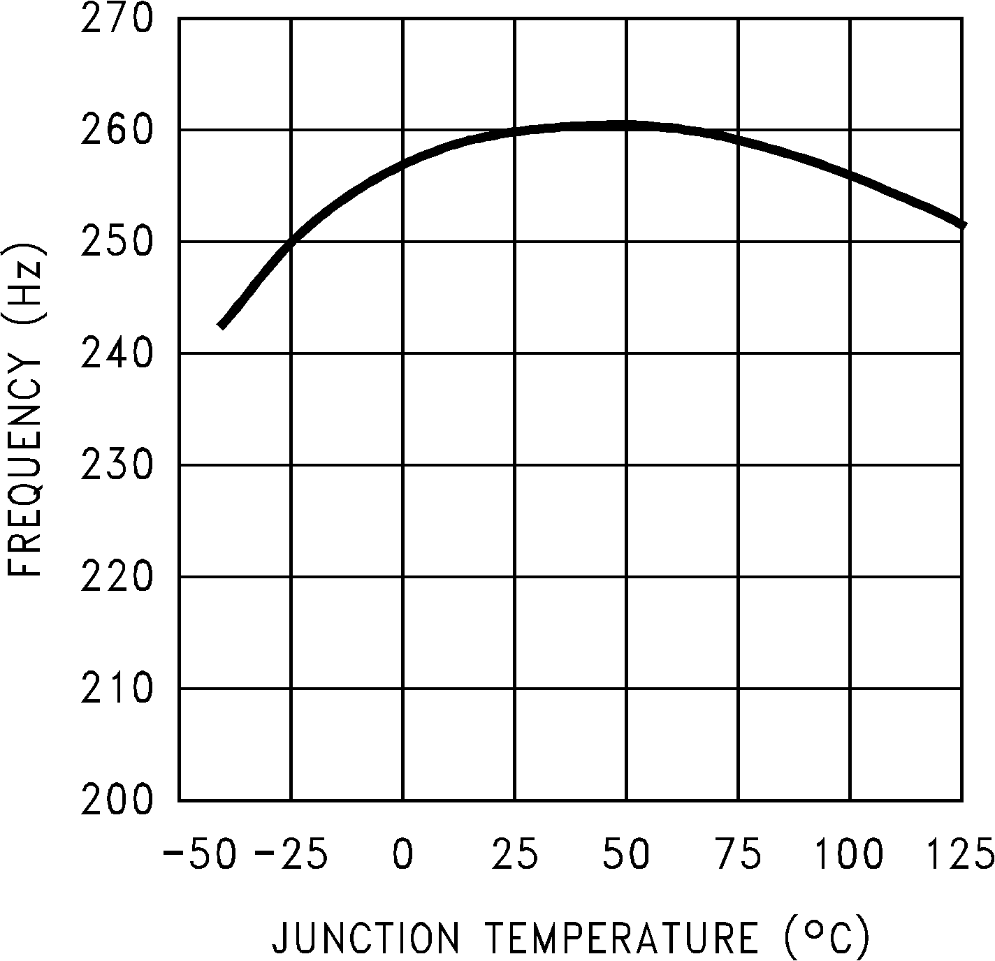 Figure 7. Switching Frequency
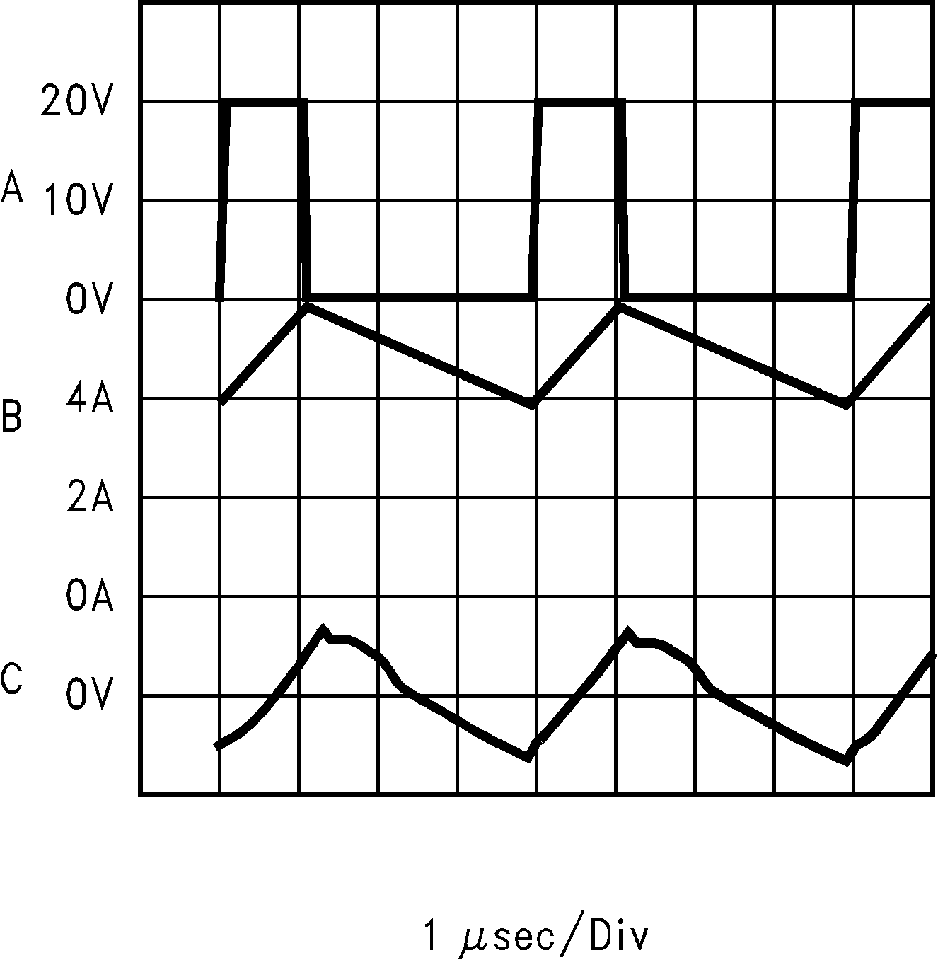
Continuous Mode Switching Waveforms VIN = 20 V, VOUT = 5 V,
ILOAD = 5 A, L = 10 μH, COUT = 400 μF, COUTESR = 13 mΩ
A. VSW pin voltage, 10 V/div
B. Inductor current, 2 A/div
C. Output ripple voltage, 20 mV/div AC-coupled
Figure 9. Horizontal Time Base: 1 μs/div
ILOAD = 5 A, L = 10 μH, COUT = 400 μF, COUTESR = 13 mΩ
A. VSW pin voltage, 10 V/div
B. Inductor current, 2 A/div
C. Output ripple voltage, 20 mV/div AC-coupled
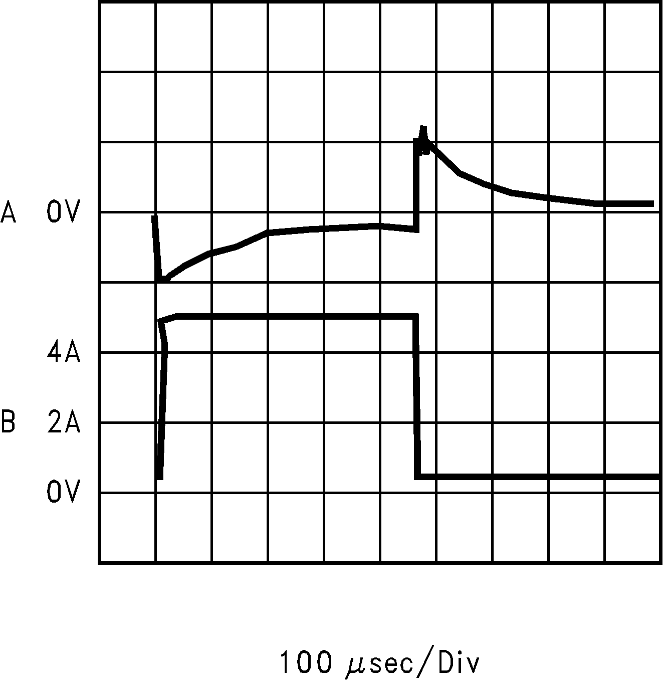
Load Transient Response for Continuous Mode VIN = 20 V,
VOUT = 5 V, L = 10 μH, COUT = 400 μF, COUTESR = 13 mΩ
A. Output voltage, 100 mV/div, AC-coupled
B. Load current: 500-mA to 5-A load pulse
Figure 11. Horizontal Time Base: 100 μs/div
VOUT = 5 V, L = 10 μH, COUT = 400 μF, COUTESR = 13 mΩ
A. Output voltage, 100 mV/div, AC-coupled
B. Load current: 500-mA to 5-A load pulse
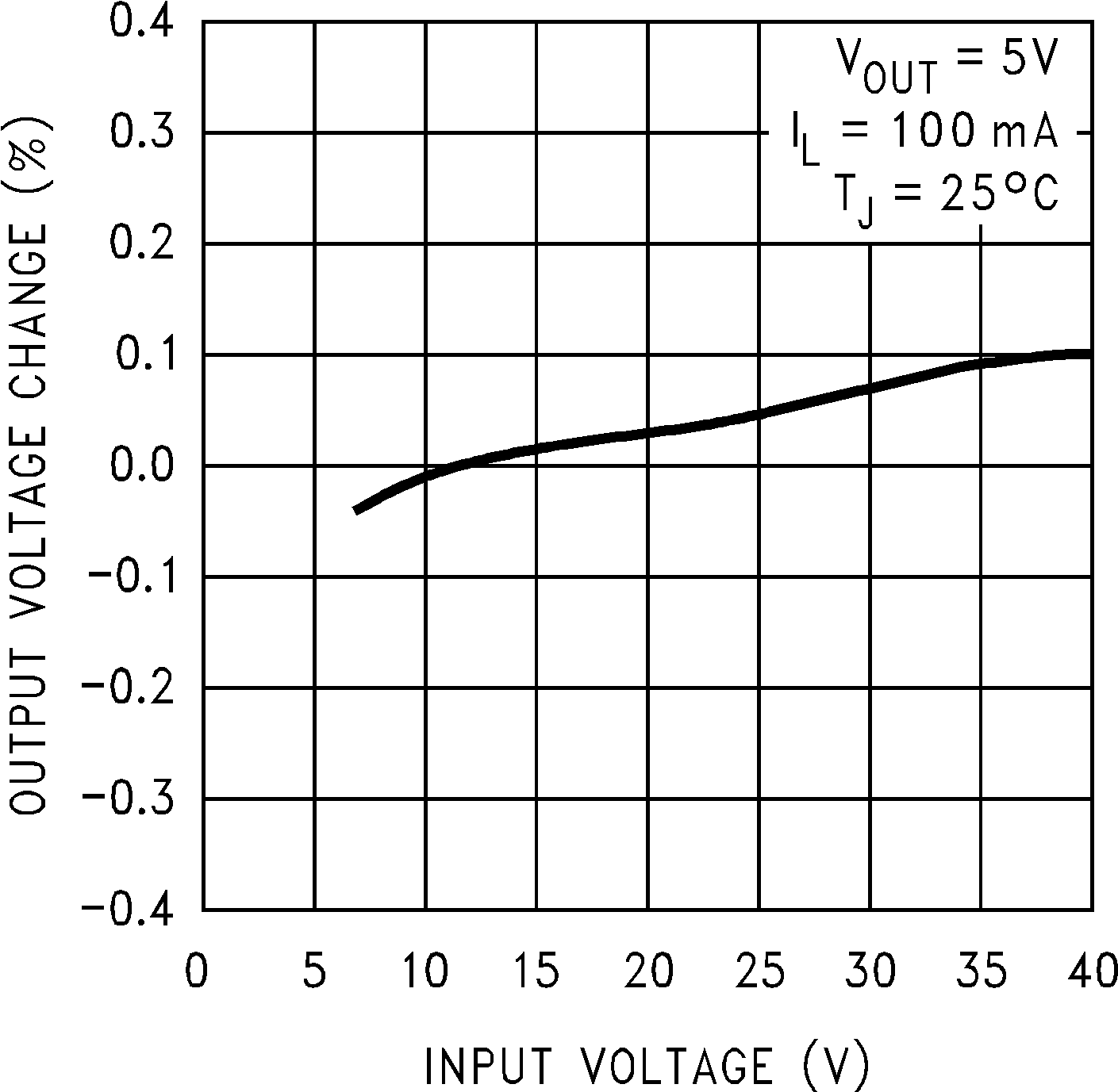 Figure 2. Line Regulation
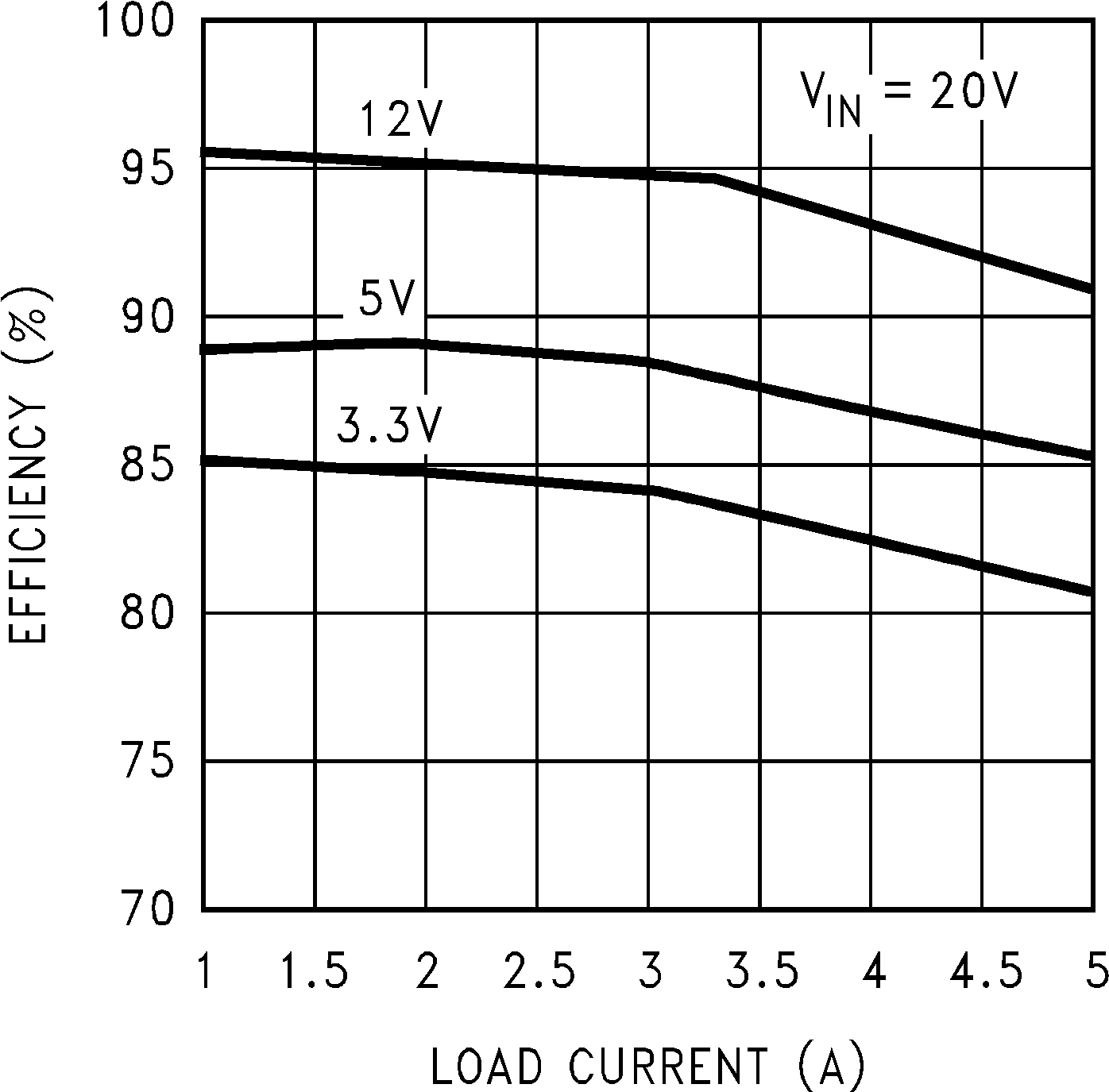 Figure 4. Efficiency vs ILOAD
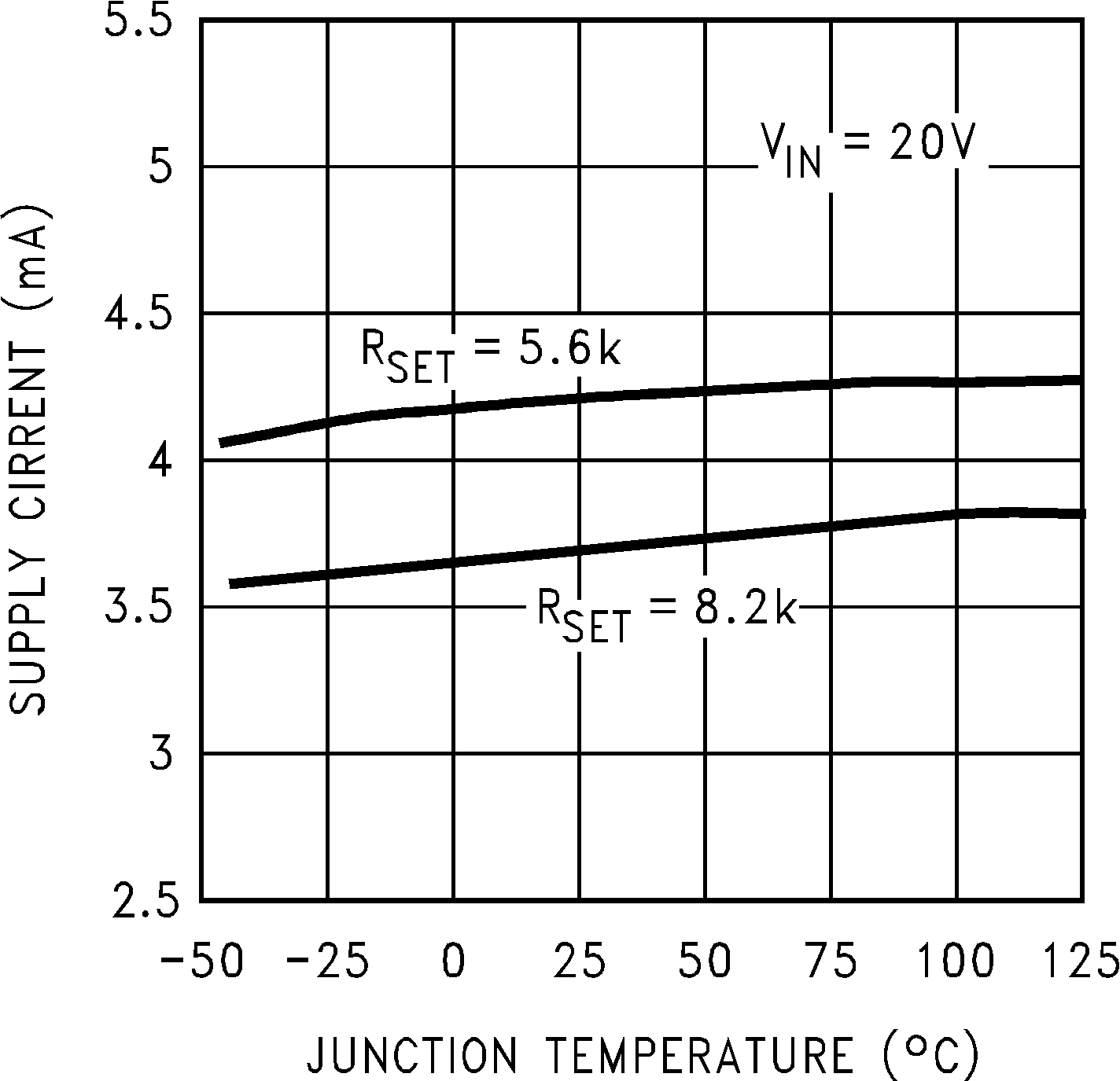 Figure 6. Operating Quiescent Current
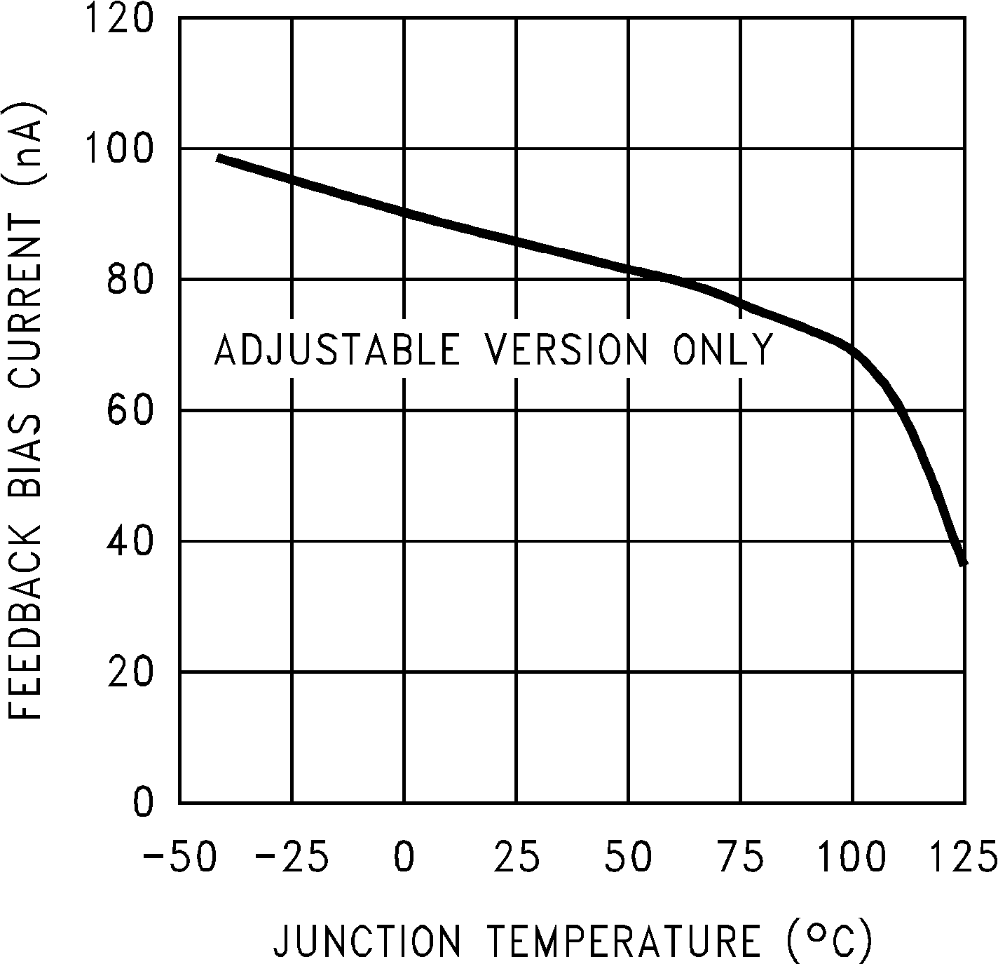 Figure 8. Feedback Pin Bias Current
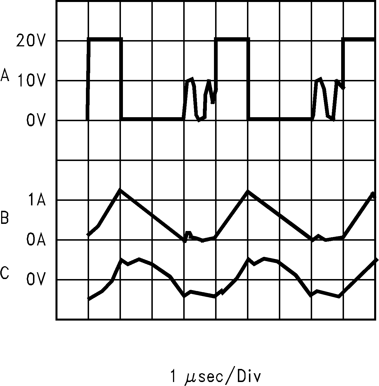
Discontinuous Mode Switching Waveforms VIN = 20 V, VOUT = 5 V,
ILOAD = 500 mA, L = 10 μH, COUT = 400 μF, COUTESR = 13 mΩ
A. VSW pin voltage, 10 V/div
B. Inductor current, 1 A/div
C. Output ripple voltage, 20 mV/div AC-coupled
Figure 10. Horizontal Time Base: 1 μs/div
ILOAD = 500 mA, L = 10 μH, COUT = 400 μF, COUTESR = 13 mΩ
A. VSW pin voltage, 10 V/div
B. Inductor current, 1 A/div
C. Output ripple voltage, 20 mV/div AC-coupled
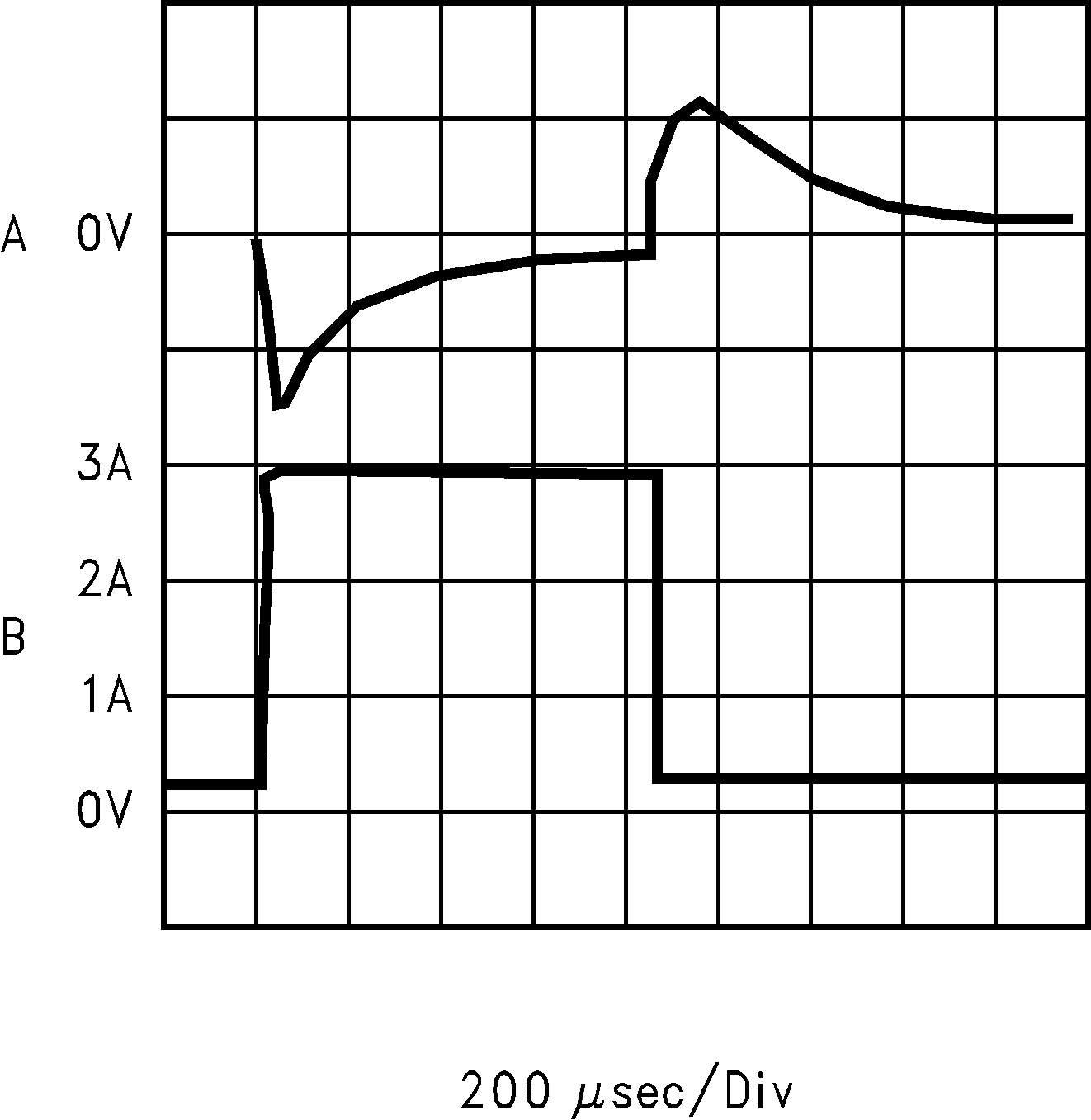
Load Transient Response for Discontinuous Mode VIN = 20 V,
VOUT = 5 V, L = 10 μH, COUT = 400 μF, COUTESR = 13 mΩ
A. Output voltage, 100 mV/div, AC-coupled
B. Load current: 200-mA to 3-A load pulse
Figure 12. Horizontal Time Base: 200 μs/div
VOUT = 5 V, L = 10 μH, COUT = 400 μF, COUTESR = 13 mΩ
A. Output voltage, 100 mV/div, AC-coupled
B. Load current: 200-mA to 3-A load pulse