SNVS276I April   2004  – February 2019 LM2743

PRODUCTION DATA.  

  1. Features
  2. Applications
  3. Description
    1.     Device Images
      1.      Typical Application Diagram
  4. Revision History
  5. Pin Configuration and Functions
    1.     Pin Functions
  6. Specifications
    1. 6.1 Absolute Maximum Ratings
    2. 6.2 ESD Ratings
    3. 6.3 Recommended Operating Conditions
    4. 6.4 Thermal Information
    5. 6.5 Electrical Characteristics
    6. 6.6 Typical Characteristics
  7. Detailed Description
    1. 7.1 Overview
    2. 7.2 Functional Block Diagram
    3. 7.3 Feature Description
      1. 7.3.1  Start Up and Soft-Start
      2. 7.3.2  Normal Operation
      3. 7.3.3  Tracking a Voltage Level
      4. 7.3.4  Tracking Voltage Slew Rate
      5. 7.3.5  Sequencing
      6. 7.3.6  SD Pin Impedance
      7. 7.3.7  MOSFET Gate Drivers
      8. 7.3.8  Power Good Signal
      9. 7.3.9  UVLO
      10. 7.3.10 Current Limit
      11. 7.3.11 Foldback Current Limit
    4. 7.4 Device Functional Modes
      1. 7.4.1 Shutdown
  8. Application and Implementation
    1. 8.1 Application Information
    2. 8.2 Typical Applications
      1. 8.2.1 Synchronous Buck Converter Typical Application using LM2743
        1. 8.2.1.1 Design Requirements
        2. 8.2.1.2 Detailed Design Procedure
          1. 8.2.1.2.1 Custom Design With WEBENCH® Tools
          2. 8.2.1.2.2 Duty Cycle Calculation
          3. 8.2.1.2.3 Input Capacitor
          4. 8.2.1.2.4 Output Inductor
          5. 8.2.1.2.5 Output Capacitor
          6. 8.2.1.2.6 MOSFETs
          7. 8.2.1.2.7 Support Components
          8. 8.2.1.2.8 Control Loop Compensation
          9. 8.2.1.2.9 Efficiency Calculations
        3. 8.2.1.3 Application Curves
      2. 8.2.2 Example Circuit 1
        1. 8.2.2.1 Design Requirements
        2. 8.2.2.2 Detailed Design Procedure
        3. 8.2.2.3 Bill of Materials
      3. 8.2.3 Example Circuit 2
        1. 8.2.3.1 Design Requirements
        2. 8.2.3.2 Detailed Design Procedure
        3. 8.2.3.3 Bill of Materials
      4. 8.2.4 Example Circuit 3
        1. 8.2.4.1 Design Requirements
        2. 8.2.4.2 Detailed Design Procedure
        3. 8.2.4.3 Bill of Materials
  9. Power Supply Recommendations
  10. 10Layout
    1. 10.1 Layout Guidelines
    2. 10.2 Layout Example
  11. 11Device and Documentation Support
    1. 11.1 Device Support
      1. 11.1.1 Development Support
        1. 11.1.1.1 Custom Design With WEBENCH® Tools
    2. 11.2 Receiving Notification of Documentation Updates
    3. 11.3 Community Resources
    4. 11.4 Trademarks
    5. 11.5 Electrostatic Discharge Caution
    6. 11.6 Glossary
  12. 12Mechanical, Packaging, and Orderable Information

Package Options

Mechanical Data (Package|Pins)
Thermal pad, mechanical data (Package|Pins)
Orderable Information

Duty Cycle Calculation

The complete duty cycle for a buck converter is defined with Equation 16:

Equation 16. LM2743 20095290.gif

where VSWL and VSWH are the respective forward voltage drops that develop across the low side and high side MOSFETs. Assuming the inductor ripple current is 20% to 30% of the output current, therefore:

Equation 17. VSWL = IOUT x RDS(ON)LOW (Low-Side MOSFET)
Equation 18. VSWH = IOUT x RDS(ON)HIGH (High-Side MOSFET)

To calculate the maximum duty cycle use the estimated 'hot' RDS(on) value of the MOSFETs, the minimum input voltage, and maximum load. As shown in Figure 31, the worst case maximum duty cycles of the LM2743 occurs at 125°C junction temperature vs VCC (IC control section voltage). Ensure that the operating duty cycle is below the curve in Figure 31, if this condition is not satisfied, the system will be unable to develop the required duty cycle to derive the necessary system power and so the output voltage will fall out of regulation.
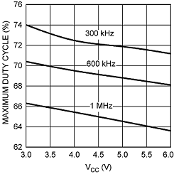
LM2743 20095291-2.pngFigure 31. Maximum Duty Cycle vs VCC
TJ = 125°C