SNVSAH6C June   2018  – May 2021 LM2775-Q1

PRODUCTION DATA  

  1. Features
  2. Applications
  3. Description
  4. Revision History
  5. Pin Configuration and Functions
  6. Specifications
    1. 6.1 Absolute Maximum Ratings
    2. 6.2 ESD Ratings
    3. 6.3 Recommended Operating Conditions
    4. 6.4 Thermal Information
    5. 6.5 Electrical Characteristics
    6. 6.6 Switching Characteristics
    7. 6.7 Typical Characteristics
  7. Detailed Description
    1. 7.1 Overview
    2. 7.2 Functional Block Diagram
    3. 7.3 Feature Description
      1. 7.3.1 Pre-Regulation
      2. 7.3.2 Input Current Limit
      3. 7.3.3 PFM Mode
      4. 7.3.4 Output Discharge
      5. 7.3.5 Thermal Shutdown
      6. 7.3.6 Undervoltage Lockout
    4. 7.4 Device Functional Modes
      1. 7.4.1 Shutdown
      2. 7.4.2 Boost Mode
  8. Application and Implementation
    1. 8.1 Application Information
    2. 8.2 Typical Application
      1. 8.2.1 Design Requirements
      2. 8.2.2 Detailed Design Procedure
        1. 8.2.2.1 Output Current Capability
        2. 8.2.2.2 Efficiency
        3. 8.2.2.3 Power Dissipation
        4. 8.2.2.4 Recommended Capacitor Types
        5. 8.2.2.5 Output Capacitor and Output Voltage Ripple
        6. 8.2.2.6 Input Capacitor and Input Voltage Ripple
        7. 8.2.2.7 Flying Capacitor
      3. 8.2.3 Application Curve
      4. 8.2.4 USB OTG / Mobile HDMI Power Supply
        1. 8.2.4.1 Design Requirements
        2. 8.2.4.2 Detailed Design Procedure
        3. 8.2.4.3 Application Curve
  9. Power Supply Recommendations
  10. 10Layout
    1. 10.1 Layout Guidelines
    2. 10.2 Layout Example
  11. 11Device and Documentation Support
    1. 11.1 Receiving Notification of Documentation Updates
    2. 11.2 Support Resources
    3. 11.3 Trademarks
    4. 11.4 Electrostatic Discharge Caution
    5. 11.5 Glossary
  12. 12Mechanical, Packaging, and Orderable Information

Package Options

Mechanical Data (Package|Pins)
Thermal pad, mechanical data (Package|Pins)
Orderable Information

Power Dissipation

LM2775-Q1 power dissipation (PD) is calculated simply by subtracting output power from input power:

Equation 5. PD = PIN – POUT = [VIN × (2 × IOUT + IQ)] – [VOUT × IOUT]

Power dissipation increases with increased input voltage and output current, up to 1.35 W at the ends of the operating ratings (VIN = 5.5 V, IOUT = 200 mA). Internal power dissipation self-heats the device. Dissipating this amount power/heat so the LM2775-Q1 does not overheat is a demanding thermal requirement for a small surface-mount package. When soldered to a PCB with layout conducive to power dissipation, the excellent thermal properties of the WSON package enable this power to be dissipated from the LM2775-Q1 with little or no derating, even when the circuit is placed in elevated ambient temperatures.
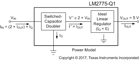
GUID-447A2E99-273E-438A-BF3B-F1BA8DA3DA1B-low.gifFigure 8-3 Power Model