SLVS075J April 1989 – January 2015 LM285-1.2 , LM385-1.2 , LM385B-1.2
PRODUCTION DATA.
- 1 Features
- 2 Applications
- 3 Description
- 4 Simplified Schematic
- 5 Revision History
- 6 Pin Configuration and Functions
- 7 Specifications
- 8 Detailed Description
- 9 Application and Implementation
- 10Power Supply Recommendations
- 11Layout
- 12Device and Documentation Support
- 13Mechanical, Packaging, and Orderable Information
Package Options
Refer to the PDF data sheet for device specific package drawings
Mechanical Data (Package|Pins)
- D|8
- LP|3
Thermal pad, mechanical data (Package|Pins)
Orderable Information
6 Pin Configuration and Functions
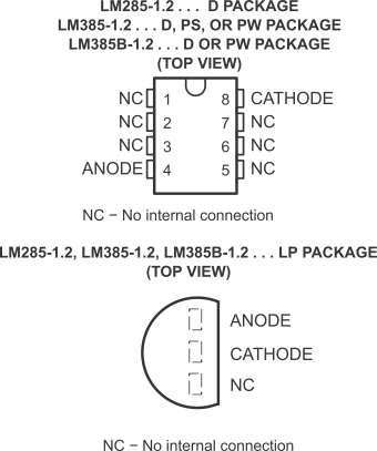
Pin Functions
| PIN | TYPE | DESCRIPTION | ||
|---|---|---|---|---|
| NAME | LP | D, PS or PW | ||
| ANODE | 1 | 4 | I | Shunt Current/Voltage input |
| CATHODE | 2 | 8 | O | Common pin, normally connected to ground |
| NC | 3 | 1, 2, 3, 5, 6, 7 | — | No internal connection |