SNVSB33 May   2018 LM3102-Q1

PRODUCTION DATA.  

  1. Features
  2. Applications
  3. Description
    1.     Device Images
      1.      Typical Application Schematic
      2.      Efficiency vs Load Current (VOUT = 3.3 V)
  4. Revision History
  5. Pin Configuration and Functions
    1.     Pin Functions
  6. Specifications
    1. 6.1 Absolute Maximum Ratings
    2. 6.2 ESD Ratings
    3. 6.3 Recommended Operating Conditions
    4. 6.4 Thermal Information
    5. 6.5 Electrical Characteristics
    6. 6.6 Switching Characteristics
    7. 6.7 Typical Characteristics
  7. Detailed Description
    1. 7.1 Overview
    2. 7.2 Functional Block Diagram
    3. 7.3 Feature Description
      1. 7.3.1  COT Control Circuit Overview
      2. 7.3.2  Start-Up Regulator (VCC)
      3. 7.3.3  Regulation Comparator
      4. 7.3.4  Zero Coil Current Detect
      5. 7.3.5  Overvoltage Comparator
      6. 7.3.6  Current Limit
      7. 7.3.7  N-Channel MOSFET and Driver
      8. 7.3.8  Soft Start
      9. 7.3.9  Thermal Protection
      10. 7.3.10 Thermal Derating
    4. 7.4 Device Functional Modes
      1. 7.4.1 ON-Time Timer, Shutdown
  8. Application and Implementation
    1. 8.1 Application Information
    2. 8.2 Typical Application
      1. 8.2.1 Design Requirements
      2. 8.2.2 Detailed Design Procedure
        1. 8.2.2.1 Custom Design With WEBENCH® Tools
        2. 8.2.2.2 Design Steps for the LM3102-Q1 Application
        3. 8.2.2.3 External Components
      3. 8.2.3 Application Curve
    3. 8.3 System Examples
  9. Power Supply Recommendations
  10. 10Layout
    1. 10.1 Layout Guidelines
    2. 10.2 Layout Example
  11. 11Device and Documentation Support
    1. 11.1 Device Support
      1. 11.1.1 Development Support
        1. 11.1.1.1 Custom Design With WEBENCH® Tools
    2. 11.2 Receiving Notification of Documentation Updates
    3. 11.3 Community Resources
    4. 11.4 Trademarks
    5. 11.5 Electrostatic Discharge Caution
    6. 11.6 Glossary
  12. 12Mechanical, Packaging, and Orderable Information

Package Options

Mechanical Data (Package|Pins)
Thermal pad, mechanical data (Package|Pins)
Orderable Information

ON-Time Timer, Shutdown

The ON-time of the LM3102-Q1 main MOSFET is determined by the resistor RON and the input voltage VIN. It is calculated as follows:

Equation 5. LM3102-Q1 30021323.gif

The inverse relationship of ton and VIN gives a nearly constant frequency as VIN is varied. RON should be selected such that the ON-time at maximum VIN is greater than 150 ns. The ON-timer has a limiter to ensure a minimum of 150 ns for ton. This limits the maximum operating frequency, which is governed by Equation 6:

Equation 6. LM3102-Q1 30021324.gif

The LM3102-Q1 can be remotely shutdown by pulling the voltage of the EN pin below 1 V. In this shutdown mode, the SS pin is internally grounded, the ON-timer is disabled, and bias currents are reduced. Releasing the EN pin allows normal operation to resume because the EN pin is internally pulled up.
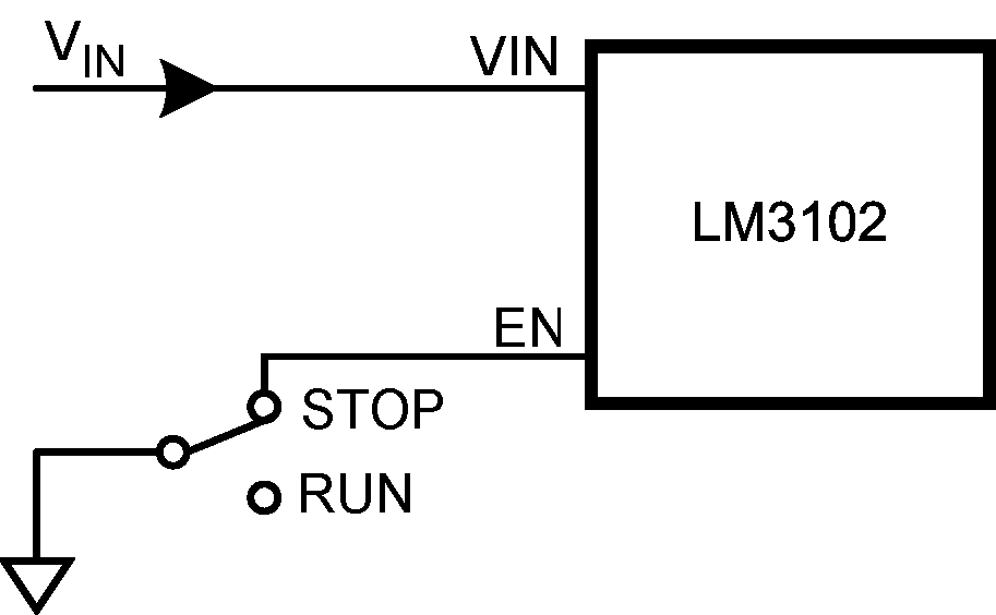
LM3102-Q1 30021325.pngFigure 22. Shutdown Implementation