SNVS429C October 2006 – December 2016 LM3405
PRODUCTION DATA.
- 1 Features
- 2 Applications
- 3 Description
- 4 Revision History
- 5 Pin Configuration and Functions
- 6 Specifications
- 7 Detailed Description
-
8 Application and Implementation
- 8.1 Application Information
- 8.2 Typical Applications
- 8.3
System Examples
- 8.3.1 VBOOST Derived From VOUT (VIN = 12 V, IF = 1 A)
- 8.3.2 VBOOST Derived From VIN Through a Series Zener Diode, D3 (VIN = 15 V, IF = 1 A)
- 8.3.3 VBOOST Derived From VIN Through a Shunt Zener Diode, D3 (VIN = 15 V, IF = 1 A)
- 8.3.4 VBOOST Derived from VOUT Through a Series Zener Diode, D3 (VIN = 15 V, IF = 1 A)
- 9 Power Supply Recommendations
- 10Layout
- 11Device and Documentation Support
- 12Mechanical, Packaging, and Orderable Information
Package Options
Mechanical Data (Package|Pins)
- DDC|6
Thermal pad, mechanical data (Package|Pins)
Orderable Information
10 Layout
10.1 Layout Guidelines
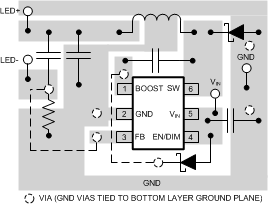
When planning the layout there are a few things to consider when trying to achieve a clean, regulated output. The most important consideration when completing the layout is the close coupling of the GND connections of the input capacitor C1 and the catch diode D1. These ground ends must be close to one another and be connected to the GND plane with at least two vias. Place these components as close to the IC as possible. The next consideration is the location of the GND connection of the output capacitor C2, which must be near the GND connections of C1 and D1.
There must be a continuous ground plane on the bottom layer of a two-layer board.
The FB pin is a high impedance node and take care to make the FB trace short to avoid noise pickup that causes inaccurate regulation. The LED current setting resistor R1 must be placed as close as possible to the IC, with the GND of R1 placed as close as possible to the GND of the IC. The VOUT trace to LED anode must be routed away from the inductor and any other traces that are switching.
High AC currents flow through the VIN, SW and VOUT traces, so they must be as short and wide as possible. Radiated noise can be decreased by choosing a shielded inductor.
The remaining components must also be placed as close as possible to the IC. See AN-1229 SIMPLE SWITCHER® PCB Layout Guidelines (SNVA054) for further considerations.
