SNVS553C January 2008 – November 2016 LM3407
PRODUCTION DATA.
- 1 Features
- 2 Applications
- 3 Description
- 4 Revision History
- 5 Pin Configuration and Functions
- 6 Specifications
- 7 Detailed Description
- 8 Application and Implementation
- 9 Power Supply Recommendations
- 10Layout
- 11Device and Documentation Support
- 12Mechanical, Packaging, and Orderable Information
Package Options
Mechanical Data (Package|Pins)
- DGN|8
Thermal pad, mechanical data (Package|Pins)
- DGN|8
Orderable Information
10 Layout
10.1 Layout Guidelines
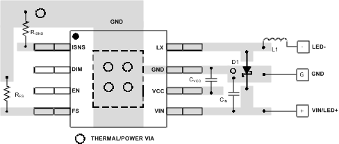
Because the copper traces of PCBs carry resistance and parasitic inductance, the longer the copper trace, the higher the resistance and inductance. These factors introduce voltage and current spikes to the switching nodes and may impair circuit performance. To optimize the performance of the LM3407, the rule of thumb is to keep the connections between components as short and direct as possible. Because true average current regulation is achieved by detecting the average switch current, the current setting resistor RISNS must be located as close as possible to the LM3407 to reduce the parasitic inductance of the copper trace and avoid noise pick-up. The connections between the LX pin, rectifier D1, inductor L1, and output capacitor COUT should be kept as short as possible to reduce the voltage spikes at the LX pin. TI recommends that CVCC, the output filter capacitor for the internal linear regulator of the LM3407, be placed close to the VCC pin. The input filter capacitor CIN should be located close to L1 and the cathode of D1. If CIN is connected to the VIN pin by a long trace, a 0.1-µF capacitor should be added close to VIN pin for noise filtering.
CAUTION
In normal operation, heat will be generated inside the LM3407 and may damage the device if no thermal management is applied. For more details on switching power supply layout considerations see AN-1149 Layout Guidelines for Switching Power Supplies (SNVA021).
