SNVS541H October 2007 – August 2016 LM3410 , LM3410-Q1
PRODUCTION DATA.
- 1 Features
- 2 Applications
- 3 Description
- 4 Revision History
- 5 Pin Configuration and Functions
- 6 Specifications
- 7 Detailed Description
-
8 Application and Implementation
- 8.1 Application Information
- 8.2
Typical Applications
- 8.2.1 Low Input Voltage, 1.6-MHz, 3 to 5 White LED Output at 50-mA Boost Converter
- 8.2.2 LM3410X SOT-23: 5 × 1206 Series LED String Application
- 8.2.3 LM3410Y SOT-23: 5 × 1206 Series LED String Application
- 8.2.4 LM3410X WSON: 7 × 5 LED Strings Backlighting Application
- 8.2.5 LM3410X WSON: 3 × HB LED String Application
- 8.2.6 LM3410Y SOT-23: 5 × 1206 Series LED String Application With OVP
- 8.2.7 LM3410X SEPIC WSON: HB or OLED Illumination Application
- 8.2.8 LM3410X WSON: Boost Flash Application
- 8.2.9 LM3410X SOT-23: 5 × 1206 Series LED String Application With VIN > 5.5 V
- 8.2.10 LM3410X WSON: Camera Flash or Strobe Circuit Application
- 8.2.11 LM3410X SOT-23: 5 × 1206 Series LED String Application With VIN and VPWR Rail > 5.5 V
- 8.2.12 LM3410X WSON: Boot-Strap Circuit to Extend Battery Life
- 9 Power Supply Recommendations
- 10Layout
- 11Device and Documentation Support
- 12Mechanical, Packaging, and Orderable Information
Package Options
Mechanical Data (Package|Pins)
Thermal pad, mechanical data (Package|Pins)
- DGN|8
Orderable Information
8 Application and Implementation
NOTE
Information in the following applications sections is not part of the TI component specification, and TI does not warrant its accuracy or completeness. TI’s customers are responsible for determining suitability of components for their purposes. Customers should validate and test their design implementation to confirm system functionality.
8.1 Application Information
8.1.1 Boost Converter
8.1.1.1 Setting the LED Current
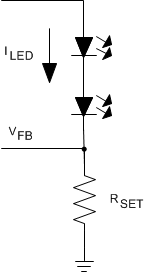 Figure 12. Setting ILED
The LED current is set using the following equation:

where
- RSET is connected between the FB pin and GND.
8.1.1.2 LED-Drive Capability
When using the LM3410 or LM3410-Q1 in the typical application configuration, with LEDs stacked in series between the VOUT and FB pin, the maximum number of LEDs that can be placed in series is dependent on the maximum LED forward voltage (VFMAX).
When inserting a value for maximum VFMAX the LED forward voltage variation over the operating temperature range must be considered.
8.1.1.3 Inductor Selection
The inductor value determines the input ripple current. Lower inductor values decrease the physical size of the inductor, but increase the input ripple current. An increase in the inductor value decreases the input ripple current.
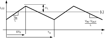 Figure 13. Inductor Current
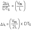
The Duty Cycle (D) for a Boost converter can be approximated by using the ratio of output voltage (VOUT) to input voltage (VIN).

Therefore:

Power losses due to the diode (D1) forward voltage drop, the voltage drop across the internal NMOS switch, the voltage drop across the inductor resistance (RDCR) and switching losses must be included to calculate a more accurate duty cycle (see Calculating Efficiency and Junction Temperature for a detailed explanation). A more accurate formula for calculating the conversion ratio is:

where
- η equals the efficiency of the device application.
Or:

Therefore:

Inductor ripple in a LED driver circuit can be greater than what would normally be allowed in a voltage regulator Boost and Sepic design. A good design practice is to allow the inductor to produce 20% to 50% ripple of maximum load. The increased ripple is unlikely to be a problem when illuminating LEDs.
From the previous equations, the inductor value is then obtained.

where
- 1 / TS = fSW
Ensure that the minimum current limit (2.1 A) is not exceeded, so the peak current in the inductor must be calculated. The peak current (Lpk I) in the inductor is calculated by Equation 10:
When selecting an inductor, make sure that it is capable of supporting the peak input current without saturating. Inductor saturation results in a sudden reduction in inductance and prevent the regulator from operating correctly. Because of the speed of the internal current limit, the peak current of the inductor only needs to be specified for the required maximum input current. For example, if the designed maximum input current is 1.5 A and the peak current is 1.75 A, then the inductor must be specified with a saturation current limit of >1.75 A. There is no need to specify the saturation or peak current of the inductor at the 2.8-A typical switch current limit.
Because of the operating frequency of the LM3410 and LM3410-Q1, ferrite based inductors are preferred to minimize core losses. This presents little restriction because the variety of ferrite-based inductors is huge. Lastly, inductors with lower series resistance (DCR) provides better operating efficiency. For recommended inductor value examples, see Typical Applications.
8.1.1.4 Input Capacitor
An input capacitor is necessary to ensure that VIN does not drop excessively during switching transients. The primary specifications of the input capacitor are capacitance, voltage, RMS current rating, and ESL (Equivalent Series Inductance). TI recommens an input capacitance from 2.2 µF to 22 µF depending on the application. The capacitor manufacturer specifically states the input voltage rating. Make sure to check any recommended deratings and also verify if there is any significant change in capacitance at the operating input voltage and the operating temperature. The ESL of an input capacitor is usually determined by the effective cross sectional area of the current path. At the operating frequencies of the LM3410 and LM3410-Q1, certain capacitors may have an ESL so large that the resulting impedance (2πfL) is higher than that required to provide stable operation. As a result, TI recommends surface mount capacitors. Multilayer ceramic capacitors (MLCC) are good choices for both input and output capacitors and have very low ESL. For MLCCs TI recommends use of X7R or X5R dielectrics. Consult the capacitor manufacturer's datasheet for rated capacitance variation over operating conditions.
8.1.1.5 Output Capacitor
The LM3410 and LM3410-Q1 operate at frequencies allowing the use of ceramic output capacitors without compromising transient response. Ceramic capacitors allow higher inductor ripple without significantly increasing output ripple. The output capacitor is selected based upon the desired output ripple and transient response. The initial current of a load transient is provided mainly by the output capacitor. The output impedance therefore determines the maximum voltage perturbation. The output ripple of the converter is a function of the capacitor’s reactance and its equivalent series resistance (ESR) (see Equation 11).

When using MLCCs, the ESR is typically so low that the capacitive ripple may dominate. When this occurs, the output ripple is approximately sinusoidal and 90° phase shifted from the switching action.
Given the availability and quality of MLCCs and the expected output voltage of designs using the LM3410 or LM3410-Q1, there no need to review any other capacitor technologies. Another benefit of ceramic capacitors is their ability to bypass high frequency noise. A certain amount of switching edge noise couples through parasitic capacitances in the inductor to the output. A ceramic capacitor bypasses this noise while a tantalum does not. Because the output capacitor is one of the two external components that control the stability of the regulator control loop, most applications requires a minimum at 0.47 µF of output capacitance. Like the input capacitor, TI recommends X7R or X5R as multilayer ceramic capacitors. Again, verify actual capacitance at the desired operating voltage and temperature.
8.1.1.6 Diode
The diode (D1) conducts during the switch off time. TI recommends Schottky diode for its fast switching times and low forward voltage drop. The diode must be chosen so that its current rating is greater than:
The reverse breakdown rating of the diode must be at least the maximum output voltage plus appropriate margin.
8.1.1.7 Output Overvoltage Protection
A simple circuit consisting of an external Zener diode can be implemented to protect the output and the LM3410 or LM3410-Q1 device from an overvoltage fault condition. If an LED fails open, or is connected backwards, an output open circuit condition occurs. No current is conducted through the LEDs, and the feedback node equals zero volts. The LM3410 or LM3410-Q1 reacts to this fault by increasing the duty cycle, thinking the LED current has dropped. A simple circuit that protects the device is shown in Figure 14.
Zener diode D2 and resistor R3 is placed from VOUT in parallel with the string of LEDs. If the output voltage exceeds the breakdown voltage of the Zener diode, current is drawn through the Zener diode, R3 and sense resistor R1. Once the voltage across R1 and R3 equals the feedback voltage of 190 mV, the LM3410 and LM3410-Q1 limits their duty cycle. No damage occurs to the device, the LEDs, or the Zener diode. Once the fault is corrected, the application will work as intended.
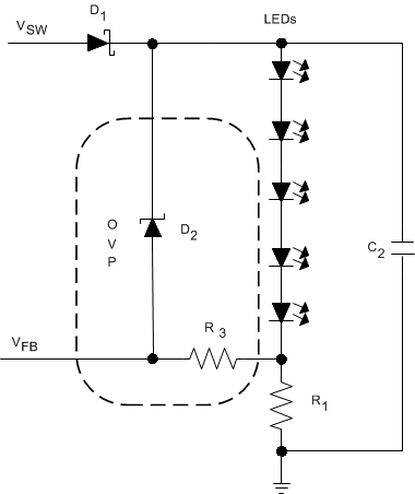 Figure 14. Overvoltage Protection Circuit
8.1.2 SEPIC Converter
The LM3410 or LM3410-Q1 can easily be converted into a SEPIC converter. A SEPIC converter has the ability to regulate an output voltage that is either larger or smaller in magnitude than the input voltage. Other converters have this ability as well (CUK and Buck-Boost), but usually create an output voltage that is opposite in polarity to the input voltage. This topology is a perfect fit for Lithium Ion battery applications where the input voltage for a single cell Li-Ion battery varies from 2.7 V to 4.5 V and the output voltage is somewhere in between. Most of the analysis of the LM3410 Boost Converter is applicable to the LM3410 SEPIC Converter.
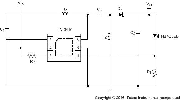 Figure 15. HB or OLED SEPIC Converter Schematic
8.1.2.1 SEPIC Equations
SEPIC Conversion ratio without loss elements:

Therefore:

Small ripple approximation:
In a well-designed SEPIC converter, the output voltage, and input voltage ripple, the inductor ripple IL1 and IL2 is small in comparison to the DC magnitude. Therefore it is a safe approximation to assume a DC value for these components. The main objective of the Steady State Analysis is to determine the steady state duty cycle, voltage and current stresses on all components, and proper values for all components.
In a steady-state converter, the net volt-seconds across an inductor after one cycle equals zero. Also, the charge into a capacitor equals the charge out of a capacitor in one cycle.
Therefore:

Substituting IL1 into IL2
The average inductor current of L2 is the average output load.
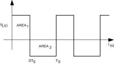 Figure 16. Inductor Volt-Second Balance Waveform
Applying Charge balance on C1:

Because there are no DC voltages across either inductor, and capacitor C3 is connected to Vin through L1 at one end, or to ground through L2 on the other end, we can say that
Therefore:

This verifies the original conversion ratio equation.
It is important to remember that the internal switch current is equal to IL1 and IL2 during the D interval. Design the converter so that the minimum ensured peak switch current limit (2.1 A) is not exceeded.
8.1.2.2 Steady State Analysis with Loss Elements
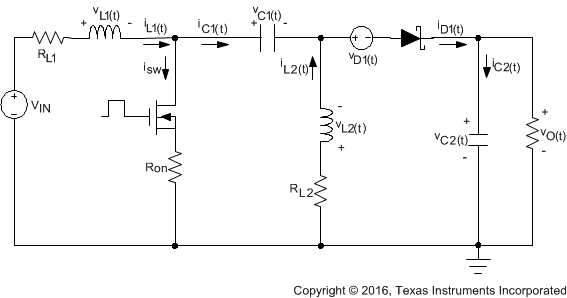 Figure 17. SEPIC Simplified Schematic
8.1.2.2.1 Details
Using inductor volt-second balance and capacitor charge balance, the following equations are derived:
and


Therefore:

All variables are known except for the duty cycle (D). A quadratic equation is needed to solve for D. A less accurate method of determining the duty cycle is to assume efficiency, and calculate the duty cycle.


Table 1. Efficiencies for Typical SEPIC Applications
| EXAMPLE 1 | EXAMPLE 2 | EXAMPLE 3 | |||
|---|---|---|---|---|---|
| VIN | 2.7 V | VIN | 3.3 V | VIN | 5 V |
| VOUT | 3.1 V | VOUT | 3.1 V | VOUT | 3.1 V |
| IIN | 770 mA | IIN | 600 mA | IIN | 375 mA |
| ILED | 500 mA | ILED | 500 mA | ILED | 500 mA |
| η | 75% | η | 80% | η | 83% |
8.2 Typical Applications
8.2.1 Low Input Voltage, 1.6-MHz, 3 to 5 White LED Output at 50-mA Boost Converter
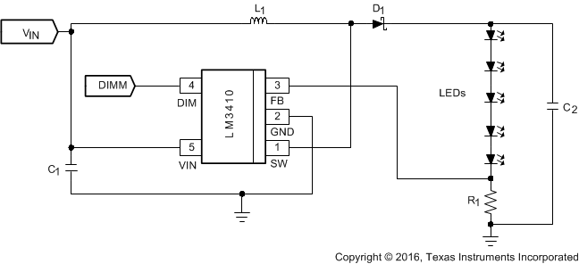 Figure 18. Boost Schematic
8.2.1.1 Design Requirements
For this design example, use the parameters listed in Table 2 as the input parameters.
Table 2. Design Parameters
| PARAMETER | EXAMPLE VALUE |
|---|---|
| VIN | 2.7 V to 5.5 V |
| ILED | 50 mA |
| VOUT | 14.6 V (four 3.6-V LEDs in series plus 190 mV) |
| RD | 8 Ω (dynamic resistance of 4 LEDs in series) |
| ΔILp–p | 100 mA (maximum) |
| ΔVOUTp–p | 250 mV (maximum) |
8.2.1.2 Detailed Design Procedure
This design procedure uses the worst-case minimum input voltage and a nominal 4 LED series load for calculations.
8.2.1.2.1 Set the LED Current (R1)
Rearranging the LED current equation the current sense resistor R1 can be found using Equation 27.

3.8 Ω is not a standard value so a standard value of R1 = 3.83 Ω is chosen.
8.2.1.2.2 Calculate Maximum Duty Cycle (DMAX)
The maximum duty cycle is required for calculating the inductor value and the minimum output capacitance. Assuming an approximate conversion efficiency (η) of 90% DMAX is calculated using Equation 28.

8.2.1.2.3 Calculate the Inductor Value (L1)
Using the maximum duty cycle, the minimum input voltage, and the maximum inductor ripple current (ΔiLp–p) the minimum inductor value to achieve the maximum ripple current is calculated using Equation 29.

To ensure the maximum inductor ripple current requirement is met with a 20% inductor tolerance an inductor value of L1 = 10 µH is selected.
8.2.1.2.4 Calculate the Output Capacitor (C2)
To maintain a maximum of 250-mV output voltage ripple the dynamic resistance of the LED stack (RD) must be used. Assuming a ceramic capacitor is used so the ESR can be neglected this minimum amount of capacitance can be found using Equation 30.

1.9 µF is not a standard value so a value of C2 = 2.2 µF is selected.
8.2.1.2.5 Input Capacitor (C1) and Schottky Diode (D1)
TI recommends an input capacitor from 2.2 µF to 22 µF. This is a relatively low power design optimized for a small footprint. For a good balance of input filtering and small size a 6.3-V capacitor with a value of C1 = 10 µF is selected. The output voltage with a 5 LED load is over 18 V and the reverse voltage of the schottky diode must be greater than this voltage. To give some headroom to avoid reverse breakdown and to maintain small size and reliability the diode selected is D1 = 30 V, 500 mA.
8.2.1.3 Application Curves
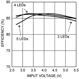 Figure 19. Efficiency versus Input Voltage
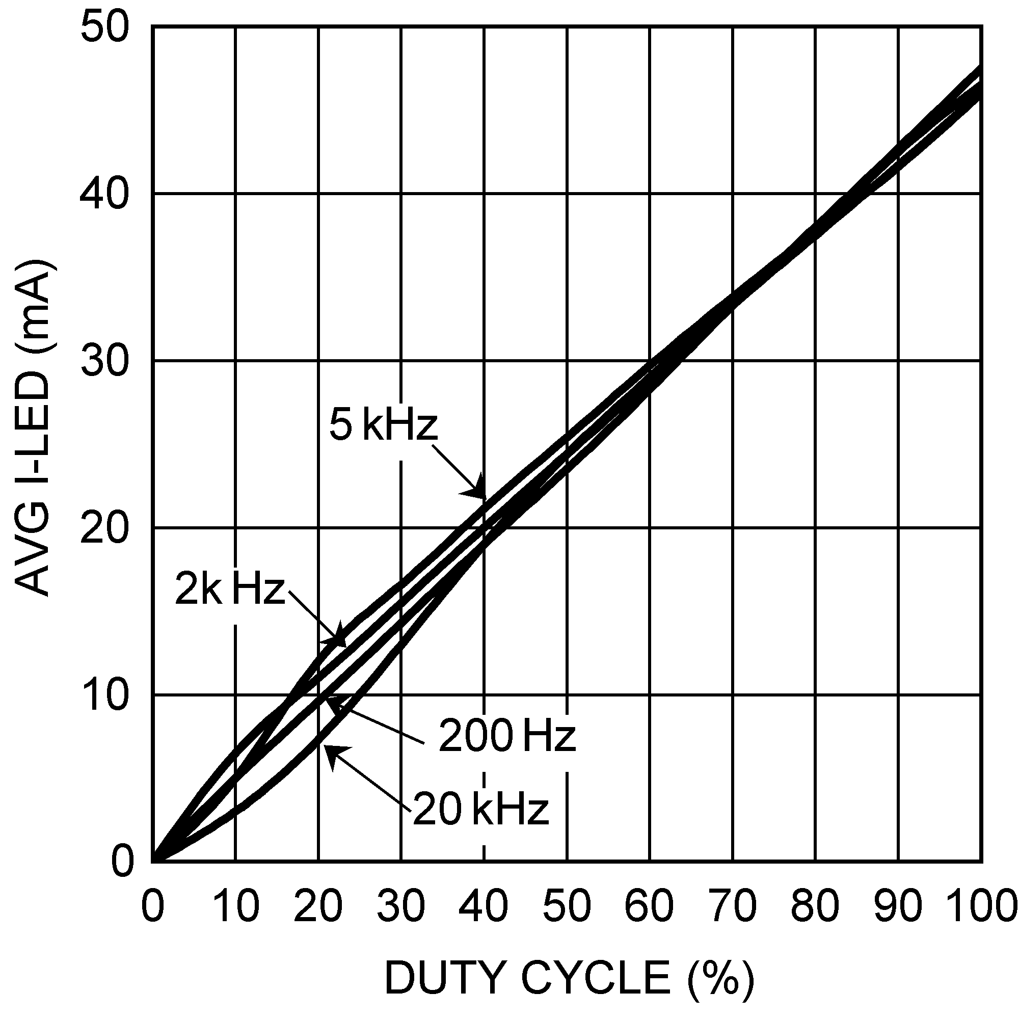 Figure 20. PWM Dimming
8.2.2 LM3410X SOT-23: 5 × 1206 Series LED String Application
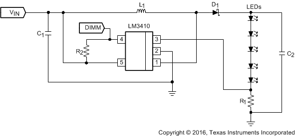 Figure 21. LM3410X (1.6 MHz) 5 × 3.3-V LED String Application Diagram
8.2.2.1 Design Requirements
For this design example, use the parameters listed in Table 3 as the input parameters.
Table 3. Design Parameters
| PARAMETER | EXAMPLE VALUE |
|---|---|
| VIN | 2.7 V to 5.5 V |
| ILED | ≊50 mA |
| VOUT | ≊16.5 V (five 3.3-V LEDs in series) |
Table 4. Part Values
| PART | VALUE |
|---|---|
| U1 | 2.8-A ISW LED Driver |
| C1, Input capacitor | 10 µF, 6.3 V, X5R |
| C2, Output capacitor | 2.2 µF, 25 V, X5R |
| D1, Catch diode | 0.4-Vf Schottky 500 mA, 30 VR |
| L1 | 10 µH, 1.2 A |
| R1 | 4.02 Ω, 1% |
| R2 | 100 kΩ, 1% |
| LEDs | SMD-1206, 50 mA, Vf ≊ 3.6 V |
8.2.3 LM3410Y SOT-23: 5 × 1206 Series LED String Application
 Figure 22. LM3410Y (525 kHz) 5 × 3.3-V LED String Application Diagram
8.2.3.1 Design Requirements
For this design example, use the parameters listed in Table 5 as the input parameters.
Table 5. Design Parameters
| PARAMETER | EXAMPLE VALUE |
|---|---|
| VIN | 2.7 V to 5.5 V |
| ILED | ≊50 mA |
| VOUT | ≊16.5 V (five 3.3-V LEDs in series) |
Table 6. Part Values
| PART | VALUE |
|---|---|
| U1 | 2.8-A ISW LED Driver |
| C1, Input capacitor | 10 µF, 6.3 V, X5R |
| C2, Output capacitor | 2.2 µF, 25 V, X5R |
| D1, Catch diode | 0.4-Vf Schottky 500 mA, 30 VR |
| L1 | 15 µH, 1.2 A |
| R1 | 4.02 Ω, 1% |
| R2 | 100 kΩ, 1% |
| LEDs | SMD-1206, 50 mA, Vf ≊ 3.6 V |
8.2.4 LM3410X WSON: 7 × 5 LED Strings Backlighting Application
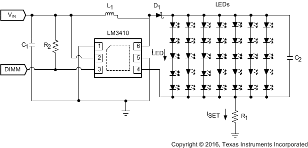 Figure 23. LM3410X (1.6 MHz) 7 × 5 × 3.3-V LEDs Backlighting Application Diagram
8.2.4.1 Design Requirements
For this design example, use the parameters listed in Table 7 as the input parameters.
Table 7. Design Parameters
| PARAMETER | EXAMPLE VALUE |
|---|---|
| VIN | 2.7 V to 5.5 V |
| ILED | ≊25 mA |
| VOUT | ≊16.7 V (seven strings of five 3.3-V LEDs in series) |
Table 8. Part Values
| PART | VALUE |
|---|---|
| U1 | 2.8-A ISW LED Driver |
| C1, Input capacitor | 10 µF, 6.3 V, X5R |
| C2, Output capacitor | 4.7 µF, 25 V, X5R |
| D1, Catch Diode | 0.4-Vf Schottky 500 mA, 30 VR |
| L1 | 8.2 µH, 2 A |
| R1 | 1.15 Ω, 1% |
| R2 | 100 kΩ, 1% |
| LEDs | SMD-1206, 50 mA, Vf ≊ 3.6 V |
8.2.5 LM3410X WSON: 3 × HB LED String Application
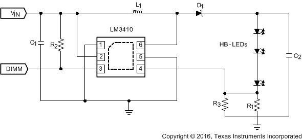 Figure 24. LM3410X (1.6 MHz) 3 × 3.4-V LED String Application Diagram
8.2.5.1 Design Requirements
For this design example, use the parameters listed in Table 9 as the input parameters.
Table 9. Design Parameters
| PARAMETER | EXAMPLE VALUE |
|---|---|
| VIN | 2.7 V to 5.5 V |
| ILED | ≊340 mA |
| VOUT | ≊11 V (three 3.4-V LEDs in series) |
Table 10. Part Values
| PART | VALUE |
|---|---|
| U1 | 2.8-A ISW LED Driver |
| C1, Input capacitor | 10 µF, 6.3 V, X5R |
| C2, Output capacitor | 2.2 µF, 25 V, X5R |
| D1, Catch diode | 0.4-Vf Schottky 500 mA, 30 VR |
| L1 | 10 µH, 1.2 A |
| R1 | 1 Ω, 1% |
| R2 | 100 kΩ, 1% |
| R3 | 1.5 Ω, 1% |
| HB – LEDs | 340 mA, Vf ≊ 3.6 V |
8.2.6 LM3410Y SOT-23: 5 × 1206 Series LED String Application With OVP
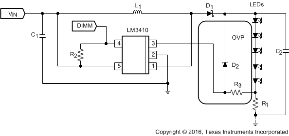 Figure 25. LM3410Y (525 kHz) 5 × 3.3-V LED String Application With OVP Diagram
8.2.6.1 Design Requirements
For this design example, use the parameters listed in Table 11 as the input parameters.
Table 11. Design Parameters
| PARAMETER | EXAMPLE VALUE |
|---|---|
| VIN | 2.7 V to 5.5 V |
| ILED | ≊50 mA |
| VOUT | ≊16.5 V (five 3.3-V LEDs in series) |
Table 12. Part Values
| PART | VALUE |
|---|---|
| U1 | 2.8-A ISW LED Driver |
| C1, Input capacitor | 10 µF, 6.3 V, X5R |
| C2, Output capacitor | 2.2 µF, 25 V, X5R |
| D1, Catch diode | 0.4-Vf Schottky 500 mA, 30 VR |
| D2 | 18 V Zener diode |
| L1 | 15 µH, 0.7 A |
| R1 | 4.02 Ω, 1% |
| R2 | 100 kΩ, 1% |
| R3 | 100 Ω, 1% |
| LEDs | SMD-1206, 50 mA, Vf ≊ 3.6 V |
8.2.7 LM3410X SEPIC WSON: HB or OLED Illumination Application
 Figure 26. LM3410X (1.6 MHz) HB or OLED Illumination Application Diagram
8.2.7.1 Design Requirements
For this design example, use the parameters listed in Table 13 as the input parameters.
Table 13. Design Parameters
| PARAMETER | EXAMPLE VALUE |
|---|---|
| VIN | 2.7 V to 5.5 V |
| ILED | ≊300 mA |
| VOUT | ≊3.8 V |
Table 14. Part Values
| PART | VALUE |
|---|---|
| U1 | 2.8-A ISW LED Driver |
| C1, Input capacitor | 10 µF, 6.3 V, X5R |
| C2, Output capacitor | 10 µF, 6.3 V, X5R |
| C3 | 2.2 µF, 25 V, X5R |
| D1, Catch diode | 0.4-Vf Schottky 1 A, 20 VR |
| L1 and L2 | 4.7 µH, 3 A |
| R1 | 665 mΩ, 1% |
| R2 | 100 kΩ, 1% |
| HB – LEDs | 350 mA, Vf ≊ 3.6 V |
8.2.8 LM3410X WSON: Boost Flash Application
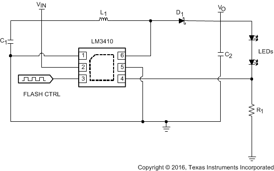 Figure 27. LM3410X (1.6 MHz) Boost Flash Application Diagram
8.2.8.1 Design Requirements
For this design example, use the parameters listed in Table 15 as the input parameters.
Table 15. Design Parameters
| PARAMETER | EXAMPLE VALUE |
|---|---|
| VIN | 2.7 V to 5.5 V |
| ILED | ≊1 A (pulse) |
| VOUT | ≊8 V |
Table 16. Part Values
| PART | VALUE |
|---|---|
| U1 | 2.8-A ISW LED Driver |
| C1, Input capacitor | 10 µF, 6.3 V, X5R |
| C2, Output capacitor | 10 µF, 16 V, X5R |
| D1, Catch diode | 0.4-Vf Schottky 500 mA, 30 VR |
| L1 | 4.7 µH, 3 A |
| R1 | 200 mΩ, 1% |
| LEDs | 500 mA, Vf ≊ 3.6 V, IPULSE = 1 A |
8.2.9 LM3410X SOT-23: 5 × 1206 Series LED String Application With VIN > 5.5 V
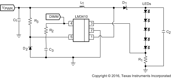 Figure 28. LM3410X (1.6 MHz) 5 × 1206 Series LED String Application With VIN > 5.5 V Diagram
8.2.9.1 Design Requirements
For this design example, use the parameters listed in Table 17 as the input parameters.
Table 17. Design Parameters
| PARAMETER | EXAMPLE VALUE |
|---|---|
| VPWR | 9 V to 14 V |
| ILED | ≊50 mA |
| VOUT | ≊16.5 V (five 3.3-V LEDs in series) |
Table 18. Part Values
| PART | VALUE |
|---|---|
| U1 | 2.8-A ISW LED Driver |
| C1, Input VPWRcapacitor | 10 µF, 6.3 V, X5R |
| C2, Output capacitor | 2.2 µF, 25 V, X5R |
| C3, Input VIN capacitor | 0.1 µF, 6.3 V, X5R |
| D1, Catch diode | 0.43-Vf Schottky 500 mA, 30 VR |
| D2 | 3.3 V Zener, SOT-23 |
| L1 | 10 µH, 1.2 A |
| R1 | 4.02 Ω, 1% |
| R2 | 100 kΩ, 1% |
| R3 | 576 Ω, 1% |
| LEDs | SMD-1206, 50 mA, Vf ≊ 3.6 V |
8.2.10 LM3410X WSON: Camera Flash or Strobe Circuit Application
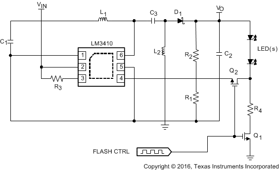 Figure 29. LM3410X (1.6 MHz) Camera Flash or Strobe Circuit Application Diagram
8.2.10.1 Design Requirements
For this design example, use the parameters listed in Table 19 as the input parameters.
Table 19. Design Parameters
| PARAMETER | EXAMPLE VALUE |
|---|---|
| VIN | 2.7 V to 5.5 V |
| ILED | ≊1.5 A (flash) |
| VOUT | ≊7.5 V |
Table 20. Part Values
| PART | VALUE |
|---|---|
| U1 | 2.8-A ISW LED Driver |
| C1, Input capacitor | 10 µF, 6.3 V, X5R |
| C2, Output capacitor | 220 µF, 10 V, tantalum |
| C3 capacitor | 10 µF, 16 V, X5R |
| D1, Catch diode | 0.43-Vf Schottky 1 A, 20 VR |
| L1 | 3.3 µH, 2.7 A |
| R1 | 1 Ω, 1% |
| R2 | 37.4 kΩ, 1% |
| R3 | 100 kΩ, 1% |
| R4 | 0.15 Ω, 1% |
| Q1 and Q2 | 30 V, ID = 3.9 A |
| LEDs | SMD-1206, 50 mA, Vf ≊ 3.6 V, IPULSE = 1.5 A |
8.2.11 LM3410X SOT-23: 5 × 1206 Series LED String Application With VIN and VPWR Rail > 5.5 V
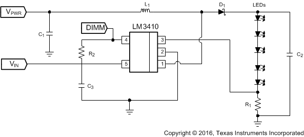 Figure 30. LM3410X (1.6 MHz) 5 × 1206 Series LED String Application With VIN and VPWR Rail > 5.5 V Diagram
8.2.11.1 Design Requirements
For this design example, use the parameters listed in Table 21 as the input parameters.
Table 21. Design Parameters
| PARAMETER | EXAMPLE VALUE |
|---|---|
| VPWR | 9 V to 14 V |
| VIN | 2.7 V to 5.5 V |
| ILED | ≊50 mA |
| VOUT | ≊16.5 V (five 3.3-V LEDs in series) |
Table 22. Part Values
| PART | VALUE |
|---|---|
| U1 | 2.8-A ISW LED Driver |
| C1, Input VPWRcapacitor | 10 µF, 6.3 V, X5R |
| C2, Output capacitor | 2.2 µF, 25 V, X5R |
| C3, Input VIN capacitor | 0.1 µF, 6.3 V, X5R |
| D1, Catch diode | 0.43-Vf Schottky 500 mA, 30 VR |
| L1 | 10 µH, 1.2 A |
| R1 | 4.02 Ω, 1% |
| R2 | 100 kΩ, 1% |
| LEDs | SMD-1206, 50 mA, Vf ≊ 3.6 V |
8.2.12 LM3410X WSON: Boot-Strap Circuit to Extend Battery Life
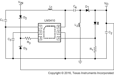 Figure 31. LM3410X (1.6 MHz) Boot-Strap Circuit to Extend Battery Life
8.2.12.1 Design Requirements
For this design example, use the parameters listed in Table 3 as the input parameters.
Table 23. Design Parameters
| PARAMETER | EXAMPLE VALUE |
|---|---|
| VIN | 1.9 V to 5.5 V |
| >2.3 V (typical) for start-up | |
| ILED | ≊300 mA |
Table 24. Part Values
| PART | VALUE |
|---|---|
| U1 | 2.8-A ISW LED Driver |
| C1, Input VPWR capacitor | 10 µF, 6.3 V, X5R |
| C2, Output capacitor | 10 µF, 6.3 V, X5R |
| C3, Input VIN capacitor | 0.1 µF, 6.3 V, X5R |
| D1, Catch diode | 0.43-Vf Schottky 1 A, 20 VR |
| D2 and D3 | Dual small signal Schottky |
| L1 and L2 | 3.3 µH, 3 A |
| R1 | 665 mΩ, 1% |
| R3 | 100 kΩ, 1% |
| HB – LEDs | 350 mA, Vf ≊ 3.4 V |