SNVS574G July 2008 – July 2019 LM3421 , LM3423
PRODUCTION DATA.
- 1 Features
- 2 Applications
- 3 Description
- 4 Revision History
- 5 Device Comparison
- 6 Pin Configuration and Functions
- 7 Specifications
-
8 Detailed Description
- 8.1 Overview
- 8.2 Functional Block Diagram
- 8.3
Feature Description
- 8.3.1 Current Regulators
- 8.3.2 Predictive Off-Time (PRO) Control
- 8.3.3 Average LED Current
- 8.3.4 Analog Dimming
- 8.3.5 Current Sense and Current Limit
- 8.3.6 Overcurrent Protection
- 8.3.7 Zero Current Shutdown
- 8.3.8 Control Loop Compensation
- 8.3.9 Start-Up Regulator
- 8.3.10 Overvoltage Lockout (OVLO)
- 8.3.11 Input Undervoltage Lockout (UVLO)
- 8.3.12 PWM Dimming
- 8.3.13 LM3423 Only: DPOL, FLT, TIMR, and LRDY
-
9 Application and Implementation
- 9.1 Application Information
- 9.2
Typical Applications
- 9.2.1
Basic Topology Schematics
- 9.2.1.1 Design Requirements
- 9.2.1.2
Detailed Design Procedure
- 9.2.1.2.1 Operating Point
- 9.2.1.2.2 Switching Frequency
- 9.2.1.2.3 Average LED Current
- 9.2.1.2.4 Inductor Ripple Current
- 9.2.1.2.5 LED Ripple Current
- 9.2.1.2.6 Peak Current Limit
- 9.2.1.2.7 Loop Compensation
- 9.2.1.2.8 Input Capacitance
- 9.2.1.2.9 N-channel FET
- 9.2.1.2.10 Diode
- 9.2.1.2.11 Output OVLO
- 9.2.1.2.12 Input UVLO
- 9.2.1.2.13 PWM Dimming Method
- 9.2.1.2.14 Analog Dimming Method
- 9.2.2
LM3421 Buck-Boost Application
- 9.2.2.1 Design Requirements
- 9.2.2.2
Detailed Design Procedure
- 9.2.2.2.1 Operating Point
- 9.2.2.2.2 Switching Frequency
- 9.2.2.2.3 Average LED Current
- 9.2.2.2.4 Inductor Ripple Current
- 9.2.2.2.5 Output Capacitance
- 9.2.2.2.6 Peak Current Limit
- 9.2.2.2.7 Loop Compensation
- 9.2.2.2.8 Input Capacitance
- 9.2.2.2.9 N-channel FET
- 9.2.2.2.10 Diode
- 9.2.2.2.11 Input UVLO
- 9.2.2.2.12 Output OVLO
- 9.2.2.3 Application Curve
- 9.2.3 LM3421 BOOST Application
- 9.2.4 LM3421 Buck-Boost Application
- 9.2.5 LM3423 Boost Application
- 9.2.6 LM3421 Buck-Boost Application
- 9.2.7 LM3423 Buck Application
- 9.2.8 LM3423 Buck-Boost Application
- 9.2.9 LM3421 SEPIC Application
- 9.2.1
Basic Topology Schematics
- 10Power Supply Recommendations
- 11Layout
- 12Device and Documentation Support
- 13Mechanical, Packaging, and Orderable Information
Package Options
Mechanical Data (Package|Pins)
- PWP|16
Thermal pad, mechanical data (Package|Pins)
- PWP|16
Orderable Information
8.3.10 Overvoltage Lockout (OVLO)
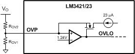
The LM3421 and LM3423 can be configured to detect an output (or input) overvoltage condition through the OVP pin. The pin features a precision 1.24-V threshold with 23 µA (typical) of hysteresis current as shown in Figure 21. When the OVLO threshold is exceeded, the GATE pin is immediately pulled low and a 23-µA current source provides hysteresis to the lower threshold of the OVLO hysteretic band.
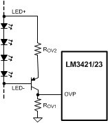
If the LEDs are referenced to a potential other than ground (floating), as in the buck-boost and buck configuration, the output voltage (VO) should be sensed and translated to ground by using a single PNP as shown in Figure 22.
The overvoltage turnoff threshold (VTURN-OFF) is defined:
Ground Referenced

Floating

In the ground referenced configuration, the voltage across ROV2 is VO – 1.24 V whereas in the floating configuration it is VO – 620 mV where 620 mV approximates VBE of the PNP.
The overvoltage hysteresis (VHYSO) is defined using Equation 25.

 Figure 21. Overvoltage Protection Circuitry
  Figure 22. Floating Output OVP Circuitry
 The OVLO feature can cause some interesting results if the OVLO trip-point is set too close to VO. At turnon, the converter has a modest amount of voltage overshoot before the control loop gains control of ILED. If the overshoot exceeds the OVLO threshold, the controller shuts down, opening the dimming MOSFET. This isolates the LED load from the converter and the output capacitance. The voltage then discharges very slowly through the HSP and HSN pins until VO drops below the lower threshold, where the process repeats. This looks like the LEDs are blinking at around 2 Hz. This mode can be escaped if the input voltage is reduced.