SNVS682D November 2010 – December 2015 LM3444
PRODUCTION DATA.
- 1 Features
- 2 Applications
- 3 Description
- 4 Revision History
- 5 Pin Configuration and Functions
- 6 Specifications
- 7 Detailed Description
-
8 Application and Implementation
- 8.1
Application Information
- 8.1.1 Determining Duty-Cycle (D)
- 8.1.2 Calculating Off-Time
- 8.1.3 Setting the Switching Frequency
- 8.1.4 Inductor Selection
- 8.1.5 Setting the LED Current
- 8.1.6 Valley Fill Capacitors
- 8.1.7 Determining the Capacitance Value of the Valley-Fill Capacitors
- 8.1.8 Determining Maximum Number of Series Connected LEDs Allowed
- 8.1.9 Output Capacitor
- 8.1.10 Switching MOSFET
- 8.1.11 Recirculating Diode
- 8.2 Typical Application
- 8.1
Application Information
- 9 Power Supply Recommendations
- 10Layout
- 11Device and Documentation Support
Package Options
Mechanical Data (Package|Pins)
Thermal pad, mechanical data (Package|Pins)
Orderable Information
5 Pin Configuration and Functions
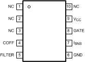
DGS Package
10-Pin VSSOP
Top View

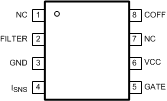
D Package
8-Lead SOIC
Top View

Pin Functions
| PIN | I/O | DESCRIPTION | ||
|---|---|---|---|---|
| NAME | VSSOP | SOIC | ||
| COFF | 4 | 8 | I | OFF time setting pin. A user set current and capacitor connected from the output to this pin sets the constant OFF time of the switching controller. |
| FILTER | 5 | 2 | I | Filter input. A low pass filter tied to this pin can filter a PWM dimming signal to supply a DC voltage to control the LED current. Can also be used as an analog dimming input. If not used for dimming connect a 0.1-µF capacitor from this pin to ground. |
| GATE | 8 | 5 | O | Power MOSFET driver pin. This output provides the gate drive for the power switching MOSFET of the buck controller. |
| GND | 6 | 3 | — | Circuit ground connection |
| ISNS | 7 | 4 | I | LED current sense pin. Connect a resistor from main switching MOSFET source, ISNS to GND to set the maximum LED current. |
| NC | 1, 2, 3, 10 | 1, 7 | — | No internal connection. Leave this pin open. |
| VCC | 9 | 6 | O | Input voltage pin. This pin provides the power for the internal control circuitry and gate driver. |