SNVS570M January 2009 – November 2015 LM3445
PRODUCTION DATA.
- 1 Features
- 2 Applications
- 3 Description
- 4 Revision History
- 5 Pin Configuration and Functions
- 6 Specifications
-
7 Detailed Description
- 7.1 Overview
- 7.2 Functional Block Diagram
- 7.3
Feature Description
- 7.3.1 Overview of Phase Control Dimming
- 7.3.2 Theory of Operation
- 7.3.3 Sensing the Rectified TRIAC Waveform
- 7.3.4 LM3445 Line Sensing Circuitry
- 7.3.5 TRIAC Holding Current Resistor
- 7.3.6 Angle Detect
- 7.3.7 Bleeder
- 7.3.8 FLTR1 Pin
- 7.3.9 Dim Decoder
- 7.3.10 Valley-Fill Circuit
- 7.3.11 Valley-Fill Operation
- 7.3.12 Buck Converter
- 7.3.13 Overview of Constant Off-Time Control
- 7.3.14 Master/Slave Operation
- 7.3.15 Master/Slave Configuration
- 7.3.16 Master Board Modifications
- 7.3.17 Slave Board Modifications
- 7.3.18 Master/Slave Interconnection
- 7.3.19 Master/Slave Theory of Operation
- 7.3.20 Master/Slave Connection Diagram
- 7.3.21 Master/Slave Block Diagrams
- 7.3.22 Thermal Shutdown
- 7.4 Device Functional Modes
-
8 Application and Implementation
- 8.1 Application Information
- 8.2 Typical Application
- 9 Power Supply Recommendations
- 10Layout
- 11Device and Documentation Support
- 12Mechanical, Packaging, and Orderable Information
Package Options
Mechanical Data (Package|Pins)
Thermal pad, mechanical data (Package|Pins)
- D|14
Orderable Information
5 Pin Configuration and Functions
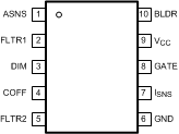
DGS Package
10-Pin VSSOP
Top View

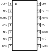
D Package
14-Pin SOIC
Top View

Pin Functions
| PIN | I/O | DESCRIPTION | ||
|---|---|---|---|---|
| NAME | SOIC | VSSOP | ||
| ASNS | 12 | 1 | O | PWM output of the TRIAC dim decoder circuit. Outputs a 0 to 4-V PWM signal with a duty cycle proportional to the TRIAC dimmer on-time. |
| BLDR | 10 | 10 | I | Bleeder pin. Provides the input signal to the angle detect circuitry as well as a current path through a switched 230-Ω resistor to ensure proper firing of the TRIAC dimmer. |
| COFF | 1 | 4 | I | OFF time setting pin. A user set current and capacitor connected from the output to this pin sets the constant OFF time of the switching controller. |
| DIM | 14 | 3 | I/O | Input/output dual function dim pin. This pin can be driven with an external PWM signal to dim the LEDs. It may also be used as an output signal and connected to the DIM pin of other LM3445s or other LED drivers to dim multiple LED circuits simultaneously. |
| FLTR1 | 13 | 2 | I | First filter input. The 120-Hz PWM signal from ASNS is filtered to a DC signal and compared to a 1 to 3 V, 5.85-kHz ramp to generate a higher frequency PWM signal with a duty cycle proportional to the TRIAC dimmer firing angle. Pull above 4.9-V (typical) to tri-state DIM. |
| FLTR2 | 3 | 5 | I | Second filter input. A capacitor tied to this pin filters the PWM dimming signal to supply a DC voltage to control the LED current. Could also be used as an analog dimming input. |
| GATE | 8 | 8 | O | Power MOSFET driver pin. This output provides the gate drive for the power switching MOSFET of the buck controller. |
| GND | 4 | 6 | — | Circuit ground connection |
| ISNS | 7 | 7 | I | LED current sense pin. Connect a resistor from main switching MOSFET source, ISNS to GND to set the maximum LED current. |
| N/C | 2, 5, 6, 11 | — | — | No Connect |
| VCC | 9 | 9 | O | Input voltage pin. This pin provides the power for the internal control circuitry and gate driver. |