SNVS085X July 2000 – December 2017 LM3478
PRODUCTION DATA.
- 1 Features
- 2 Applications
- 3 Description
- 4 Revision History
- 5 Pin Configuration and Functions
- 6 Specifications
- 7 Detailed Description
-
8 Application and Implementation
- 8.1 Application Information
- 8.2
Typical Applications
- 8.2.1
Typical High Efficiency Step-Up (Boost) Converter
- 8.2.1.1 Design Requirements
- 8.2.1.2
Detailed Design Procedure
- 8.2.1.2.1 Custom Design with WEBENCH Tools
- 8.2.1.2.2 Power Inductor Selection
- 8.2.1.2.3 Programming the Output Voltage
- 8.2.1.2.4 Setting the Current Limit
- 8.2.1.2.5 Current Limit with External Slope Compensation
- 8.2.1.2.6 Power Diode Selection
- 8.2.1.2.7 Power MOSFET Selection
- 8.2.1.2.8 Input Capacitor Selection
- 8.2.1.2.9 Output Capacitor Selection
- 8.2.1.2.10 Compensation
- 8.2.1.3 Application Curves
- 8.2.2 Typical SEPIC Converter
- 8.2.1
Typical High Efficiency Step-Up (Boost) Converter
- 9 Power Supply Recommendations
- 10Layout
- 11Device and Documentation Support
- 12Mechanical, Packaging, and Orderable Information
Package Options
Mechanical Data (Package|Pins)
Thermal pad, mechanical data (Package|Pins)
Orderable Information
7.3.3 Frequency Adjust/Shutdown
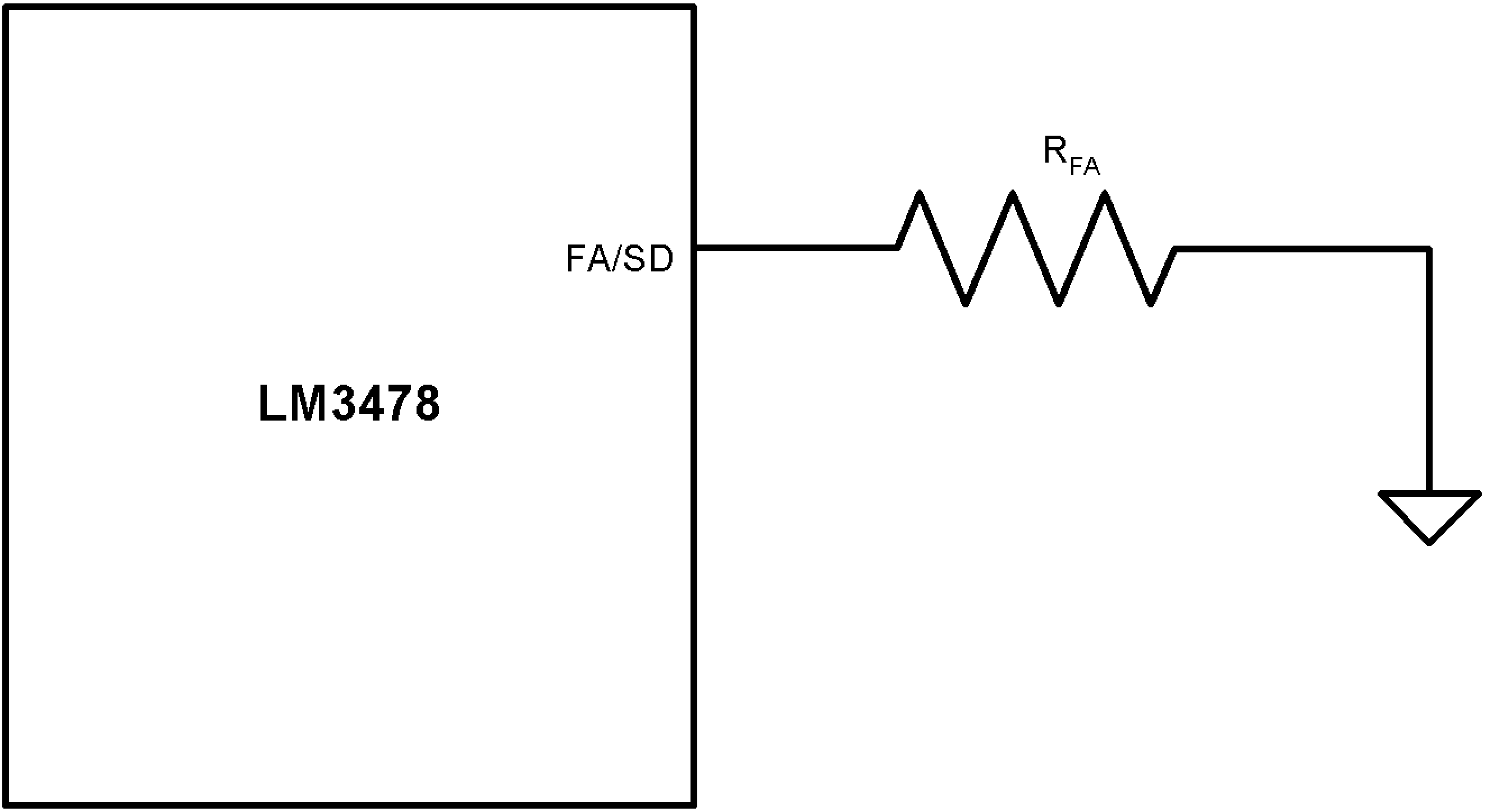
The switching frequency of the LM3478 can be adjusted between 100 kHz and 1 MHz using a single external resistor. This resistor must be connected between FA/SD pin and ground, as shown in Figure 25. To determine the value of the resistor required for a desired switching frequency, refer to Typical Characteristics or use Equation 7:
 Figure 25. Frequency Adjust
The FA/SD pin also functions as a shutdown pin. If a high signal (>1.35 V) appears on the FA/SD pin, the LM3478 stops switching and goes into a low current mode. The total supply current of the IC reduces to less than 10 µA under these conditions. Figure 26 shows implementation of the shutdown function when operating in frequency adjust mode. In this mode a high signal for more than 30 us shuts down the IC. However, the voltage on the FA/SD pin should be always less than the absolute maximum of 7 V to avoid any damage to the device.
 Figure 26. Shutdown Operation in Frequency Adjust Mode