SNVS011H June 1999 – September 2015 LM3480
PRODUCTION DATA.
- 1 Features
- 2 Applications
- 3 Description
- 4 Revision History
- 5 Pin Configuration and Functions
- 6 Specifications
- 7 Detailed Description
- 8 Application and Implementation
- 9 Power Supply Recommendations
- 10Layout
- 11Device and Documentation Support
- 12Mechanical, Packaging, and Orderable Information
Package Options
Mechanical Data (Package|Pins)
- DBZ|3
Thermal pad, mechanical data (Package|Pins)
Orderable Information
6 Specifications
6.1 Absolute Maximum Ratings(1)(2)
| MIN | MAX | UNIT | |
|---|---|---|---|
| Input voltage (IN to GND) | –0.3 | 35 | V |
| Power dissipation(3) | Internally Limited | ||
| Junction temperature(3) | –40 | 150 | °C |
| Storage temperature, Tstg | −65 | 150 | °C |
(1) Absolute Maximum Ratings are limits beyond which damage to the device may occur. Recommended Operating Conditions are conditions under which operation of the device is ensured. Recommended operating ratings do not imply ensured performance limits. For ensured performance limits and associated test conditions, see the Electrical Characteristics: LM3480-3.3, LM3480-5.
(2) If Military- or Aerospace-specified devices are required, please contact the TI Sales Office/Distributors for availability and specifications.
(3) The Absolute Maximum power dissipation depends on the ambient temperature and can be calculated using P = (TJ – TA) / RθJA where TJ is the junction temperature, TA is the ambient temperature, and RθJA is the junction-to-ambient thermal resistance. The 370-mW rating results from substituting the Absolute Maximum junction temperature, 150°C for TJ, 50°C for TA, and 269.6°C/W for RθJA. More power can be safely dissipated at lower ambient temperatures. Less power can be safely dissipated at higher ambient temperatures. The Absolute Maximum power dissipation can be increased by 3.7 mW for each °C below 50°C ambient. It must be derated by 3.7 mW for each °C above 50°C ambient. Heat sinking enables the safe dissipation of more power. The LM3480 actively limits its junction temperature to about 150°C.
6.2 ESD Ratings
| VALUE | UNIT | |||
|---|---|---|---|---|
| V(ESD) | Electrostatic discharge | Human-body model (HBM), per ANSI/ESDA/JEDEC JS-001(1) | ±2000 | V |
| Charged-device model (CDM), per JEDEC specification JESD22-C101(2) | ±500 | |||
(1) JEDEC document JEP155 states that 500-V HBM allows safe manufacturing with a standard ESD control process.
6.3 Recommended Operating Conditions
over operating free-air temperature range (unless otherwise noted)(1)| MIN | MAX | UNIT | |
|---|---|---|---|
| Maximum input voltage (IN to GND) | 0 | 30 | V |
| Junction temperature (TJ) | –40 | 125 | °C |
6.4 Thermal Information
| THERMAL METRIC(1) | LM3480 | UNIT | |
|---|---|---|---|
| SOT-23 (DBZ) | |||
| 3 PINS | |||
| RθJA | Junction-to-ambient thermal resistance | 269.6 | °C/W |
| RθJC(top) | Junction-to-case (top) thermal resistance | 141.1 | |
| RθJB | Junction-to-board thermal resistance | 63.1 | |
| ψJT | Junction-to-top characterization parameter | 24.2 | |
| ψJB | Junction-to-board characterization parameter | 62.1 | |
(1) For more information about traditional and new thermal metrics, see the IC Package Thermal Metrics application report, SPRA953.
6.5 Electrical Characteristics: LM3480-3.3, LM3480-5
Typical and other limits apply for TA = TJ = 25°C, unless otherwise specified. Nominal output voltage (VNOM) = 3.3 V or 5 V.(1)(2)(3)| PARAMETER | TEST CONDITIONS | VNOM = 3.3 V | VNOM = 5 V | UNIT | |||||
|---|---|---|---|---|---|---|---|---|---|
| MIN | TYP | MAX | MIN | TYP | MAX | ||||
| VOUT | Output voltage | VIN = VNOM + 1.5 V 1 mA ≤ IOUT ≤ 100 mA |
3.17 | 3.3 | 3.43 | 4.8 | 5 | 5.2 | V |
| VIN = VNOM + 1.5 V 1 mA ≤ IOUT ≤ 100 mA −40°C ≤ TJ ≤ 125°C |
3.14 | 3.46 | 4.75 | 5.25 | |||||
| ΔVOUT | Line regulation | VNOM + 1.5 V ≤ VIN ≤ 30 V IOUT = 1 mA |
10 | 12 | mV | ||||
| VNOM + 1.5 V ≤ VIN ≤ 30 V IOUT = 1 mA −40°C ≤ TJ ≤ 125°C |
25 | 25 | |||||||
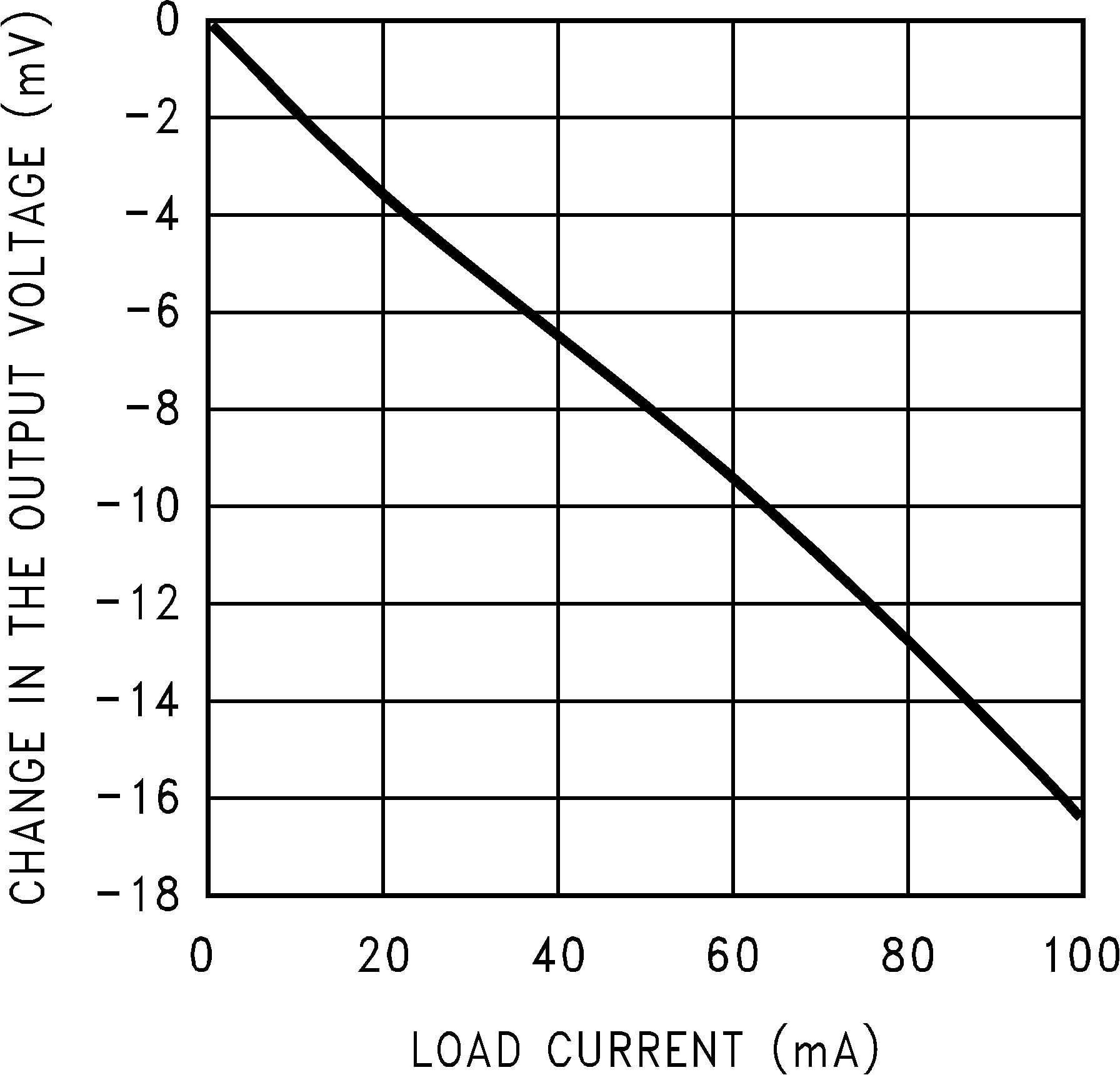
| ΔVOUT | Load regulation | VIN = VNOM + 1.5 V 10 mA ≤ IOUT ≤ 100 mA |
20 | 20 | mV | ||||
| VIN = VNOM + 1.5 V 10 mA ≤ IOUT ≤ 100 m −40°C ≤ TJ ≤ 125°C |
40 | 40 | |||||||
| IGND | Ground pin current | VNOM + 1.5 V ≤ VIN ≤ 30 V No Load |
2 | 2 | mA | ||||
| VNOM + 1.5 V ≤ VIN ≤ 30 V No Load, −40°C ≤ TJ ≤ 125°C |
4 | 4 | |||||||
| VIN - VOUT |
Dropoutvoltage | IOUT = 10 mA | 0.7 | 0.9 | 0.7 | 0.9 | V | ||
| IOUT = 10 mA −40°C ≤ TJ ≤ 125°C |
1 | 1 | |||||||
| IOUT = 100 mA | 0.9 | 1.1 | 0.9 | 1.1 | V | ||||
| IOUT = 100 mA −40°C ≤ TJ ≤ 125°C |
1.2 | 1.2 | |||||||
| en | Output noise voltage | VIN = 10 V Bandwidth: 10 Hz to 100 kHz |
100 | 150 | µVrms | ||||
(1) A typical is the center of characterization data taken with TA = TJ = 25°C. Typicals are not ensured.
(2) All limits are ensured. All electrical characteristics having room-temperature limits are tested during production with TA = TJ = 25°C. All hot and cold limits are ensured by correlating the electrical characteristics to process and temperature variations and applying statistical process control.
(3) All voltages except dropout are with respect to the voltage at the GND pin.
6.6 Electrical Characteristics: LM3480-12, LM3480-15
Typical and other limits apply for TA = TJ = 25°C, unless otherwise specified. Nominal output voltage (VNOM) = 12 V or 15 V.(1)(2)(3)| PARAMETER | TEST CONDITIONS | VNOM = 12 V | VNOM = 15 V | UNIT | |||||
|---|---|---|---|---|---|---|---|---|---|
| MIN | TYP | MAX | MIN | TYP | MAX | ||||
| VOUT | Output voltage | VIN = VNOM + 1.5 V 1 mA ≤ IOUT ≤ 100 mA |
11.52 | 12 | 12.48 | 14.4 | 15 | 15.6 | V |
| VIN = VNOM + 1.5 V 1 mA ≤ IOUT ≤ 100 mA −40°C ≤ TJ ≤ 125°C |
11.4 | 12.6 | 14.25 | 15.75 | |||||
| ΔVOUT | Line regulation | VNOM + 1.5 V ≤ VIN ≤ 30 V IOUT = 1 mA |
14 | 16 | mV | ||||
| VNOM + 1.5 V ≤ VIN ≤ 30 V IOUT = 1 mA −40°C ≤ TJ ≤ 125°C |
40 | 40 | |||||||
| ΔVOUT | Load regulation | VIN = VNOM + 1.5 V 10 mA ≤ IOUT ≤ 100 mA |
36 | 45 | mV | ||||
| VIN = VNOM + 1.5 V 10 mA ≤ IOUT ≤ 100 mA −40°C ≤ TJ ≤ 125°C |
60 | 75 | |||||||
| IGND | Ground pin current | VNOM + 1.5 V ≤ VIN ≤ 30 V No Load |
2 | 2 | mA | ||||
| VNOM + 1.5 V ≤ VIN ≤ 30 V No Load, −40°C ≤ TJ ≤ 125°C |
4 | 4 | |||||||
| VIN - VOUT |
Dropout voltage | IOUT = 10 mA | 0.7 | 0.9 | 0.7 | 0.9 | V | ||
| IOUT = 10 mA, −40°C ≤ TJ ≤ 125°C |
1 | 1 | |||||||
| IOUT = 100 mA | 0.9 | 1.1 | 0.9 | 1.1 | V | ||||
| IOUT = 100 mA , −40°C ≤ TJ ≤ 125°C |
1.2 | 1.2 | |||||||
| en | Output noise voltage | VIN = 10 V Bandwidth: 10 Hz to 100 kHz |
360 | 450 | µVrms | ||||
(1) A typical is the center of characterization data taken with TA = TJ = 25°C. Typicals are not ensured.
(2) All limits are ensured. All electrical characteristics having room-temperature limits are tested during production with TA = TJ = 25°C. All hot and cold limits are ensured by correlating the electrical characteristics to process and temperature variations and applying statistical process control.
(3) All voltages except dropout are with respect to the voltage at the GND pin.
6.7 Typical Characteristics
Unless indicated otherwise, VIN = VNOM + 1.5 V, CIN = 0.1 µF, COUT = 0.1 µF, and TA .= 25°C.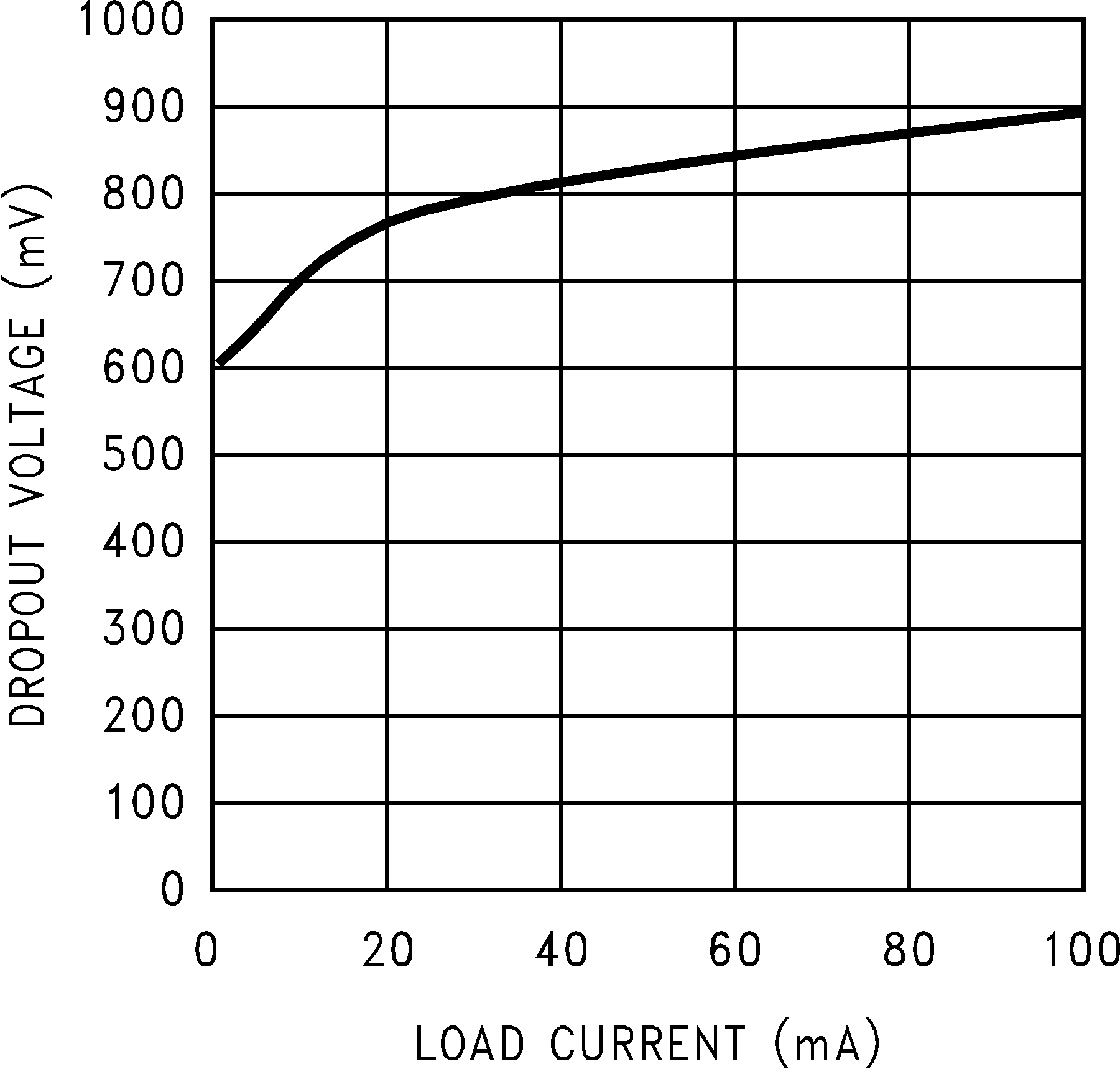 Figure 1. Dropout Voltage vs Load Current
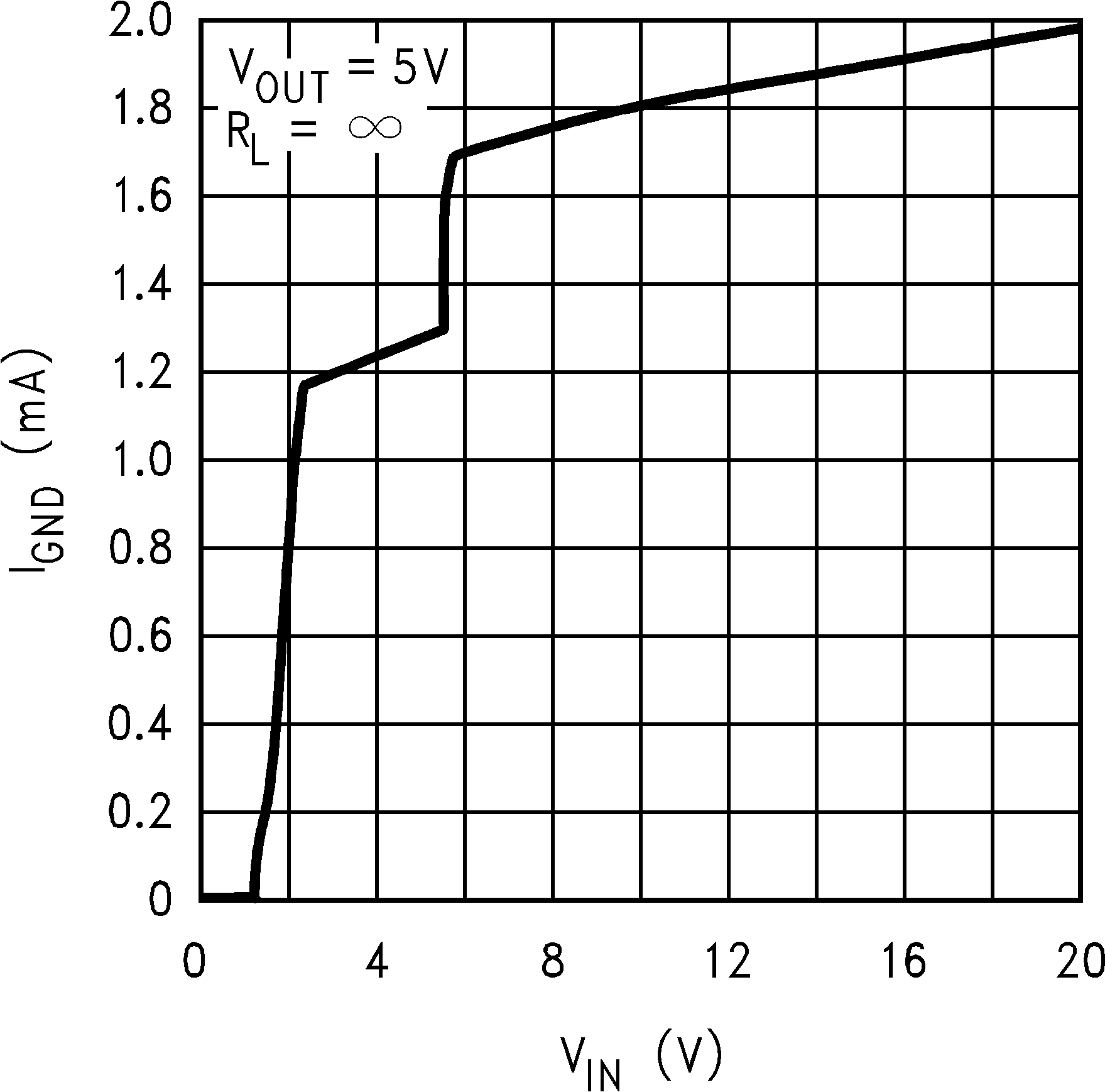 Figure 3. Ground Pin Current vs Input Voltage
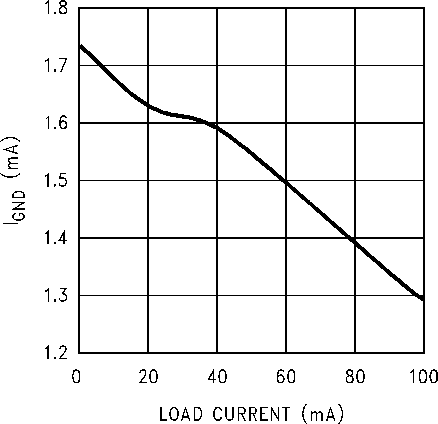 Figure 5. Ground Pin Current vs Load Current
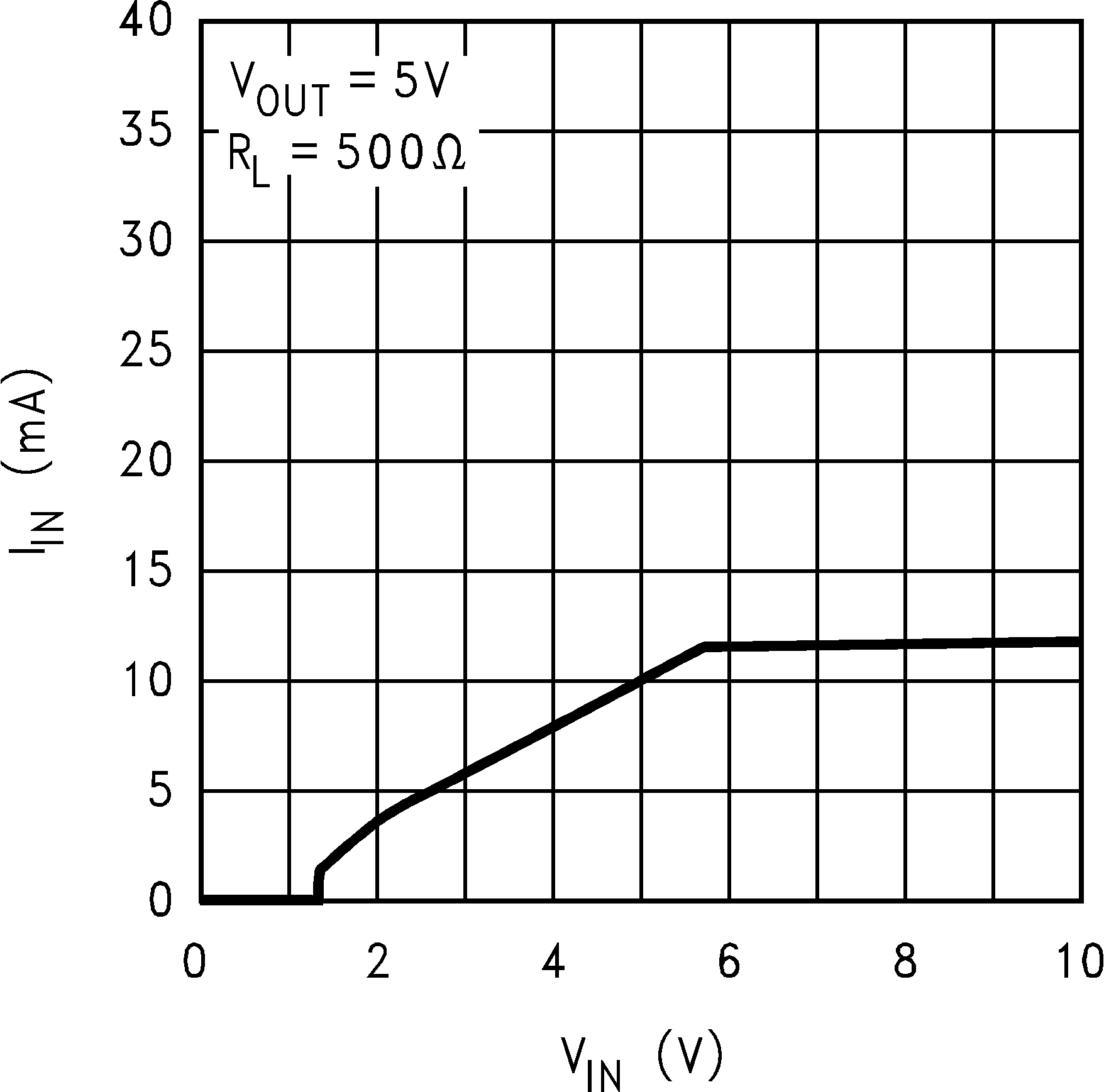 Figure 7. Input Current vs Input Voltage
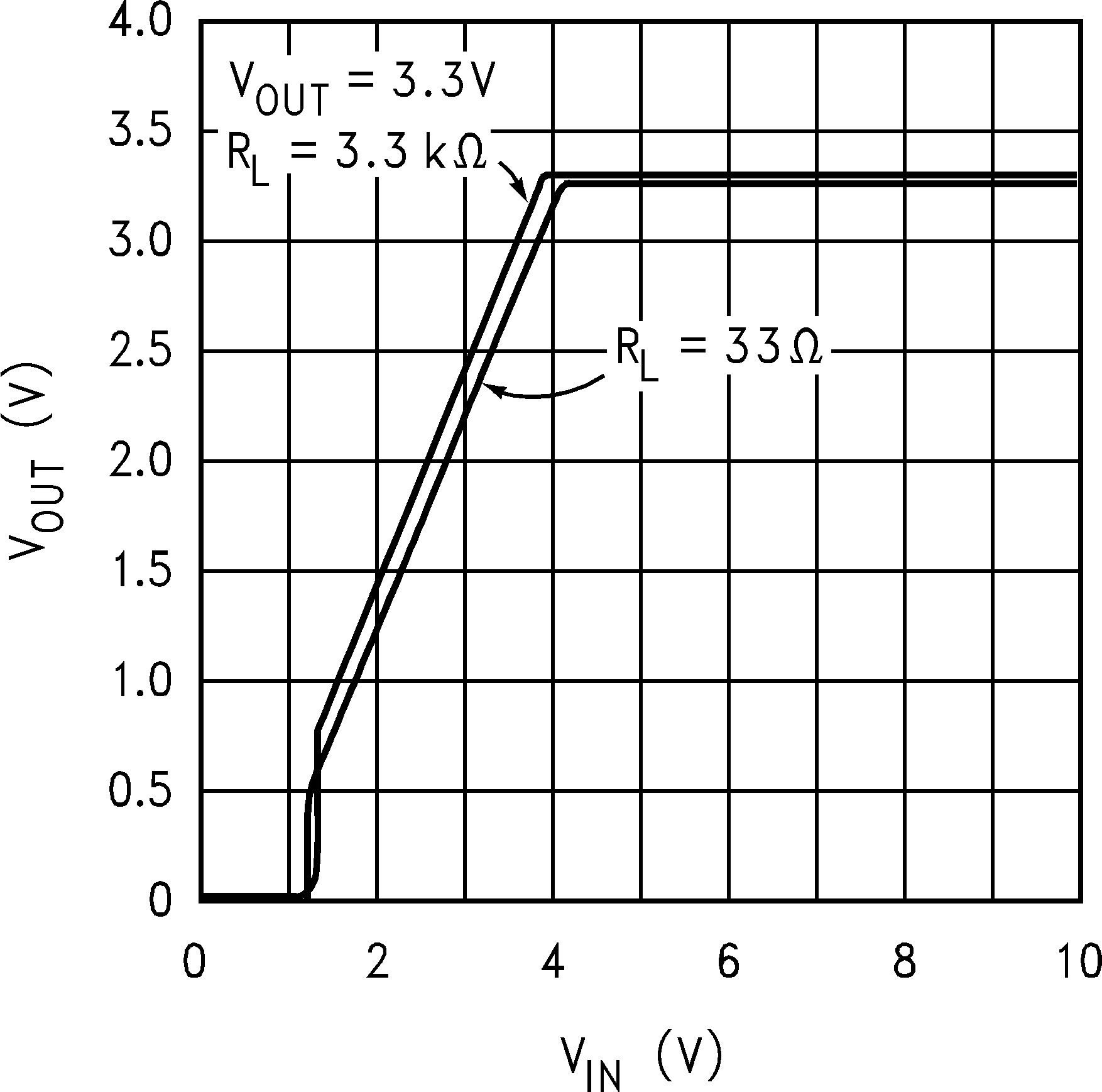 Figure 9. Output Voltage vs Input Voltage
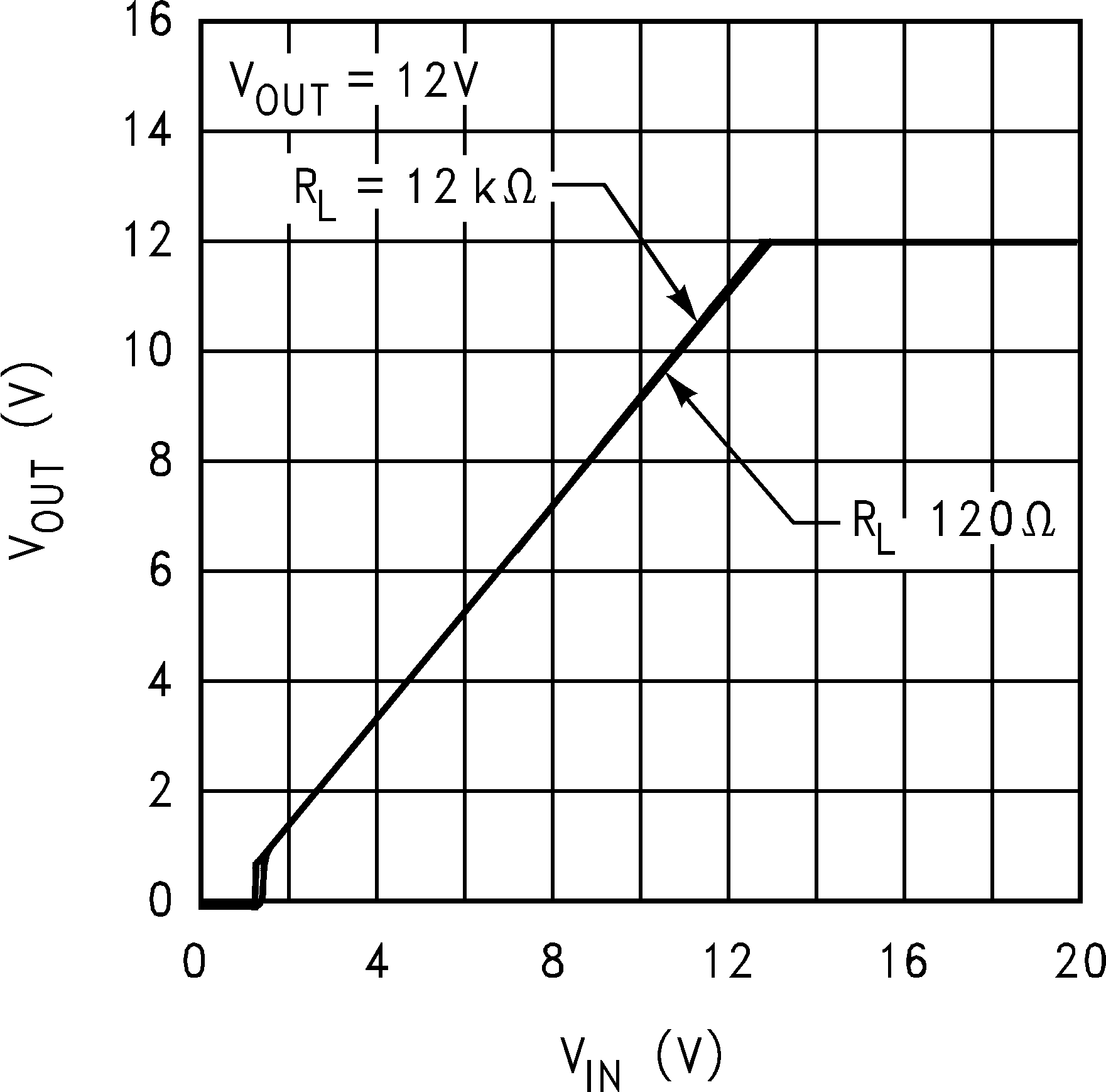 Figure 11. Output Voltage vs Input Voltage
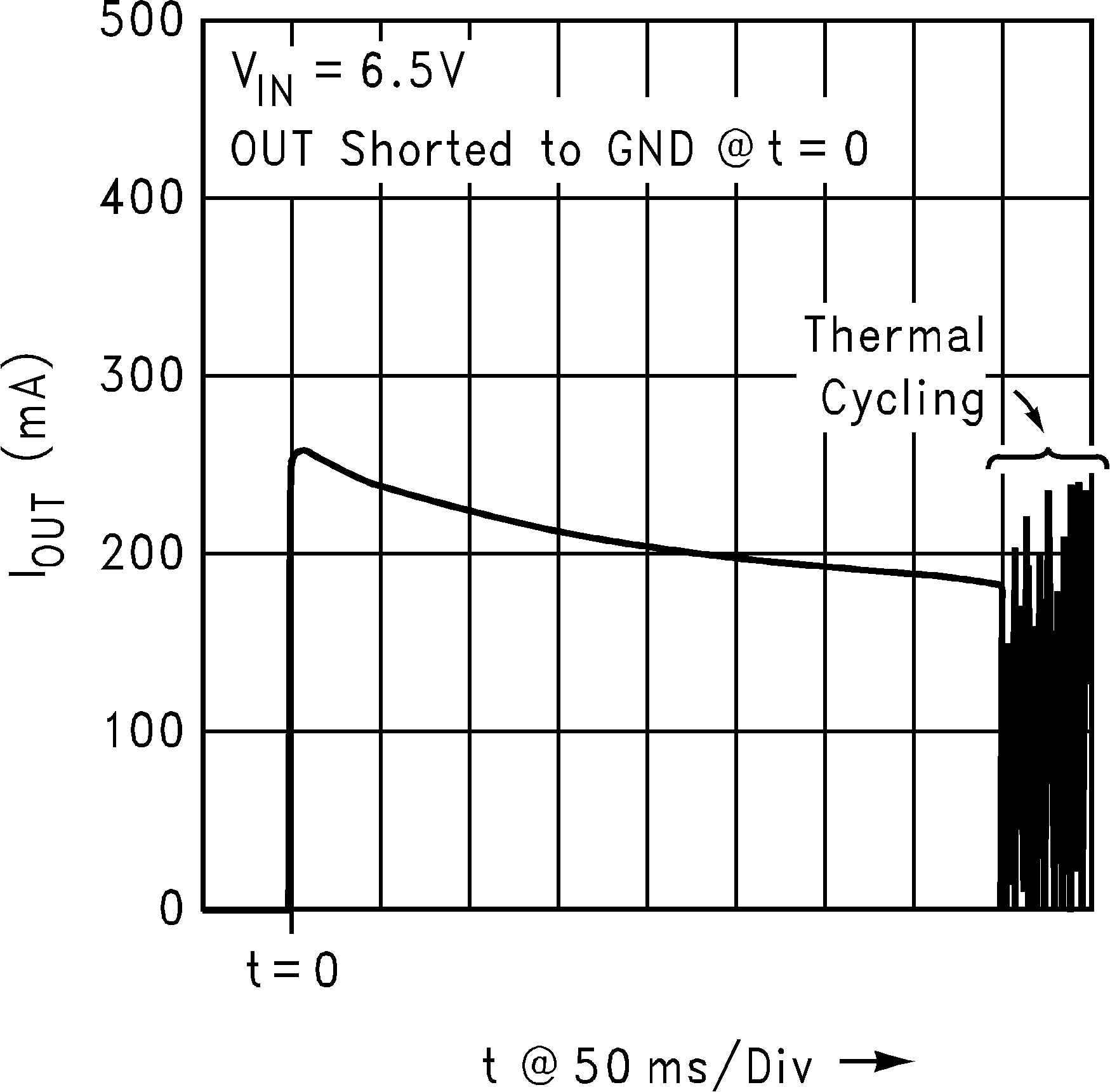 Figure 13. Output Short-Circuit Current
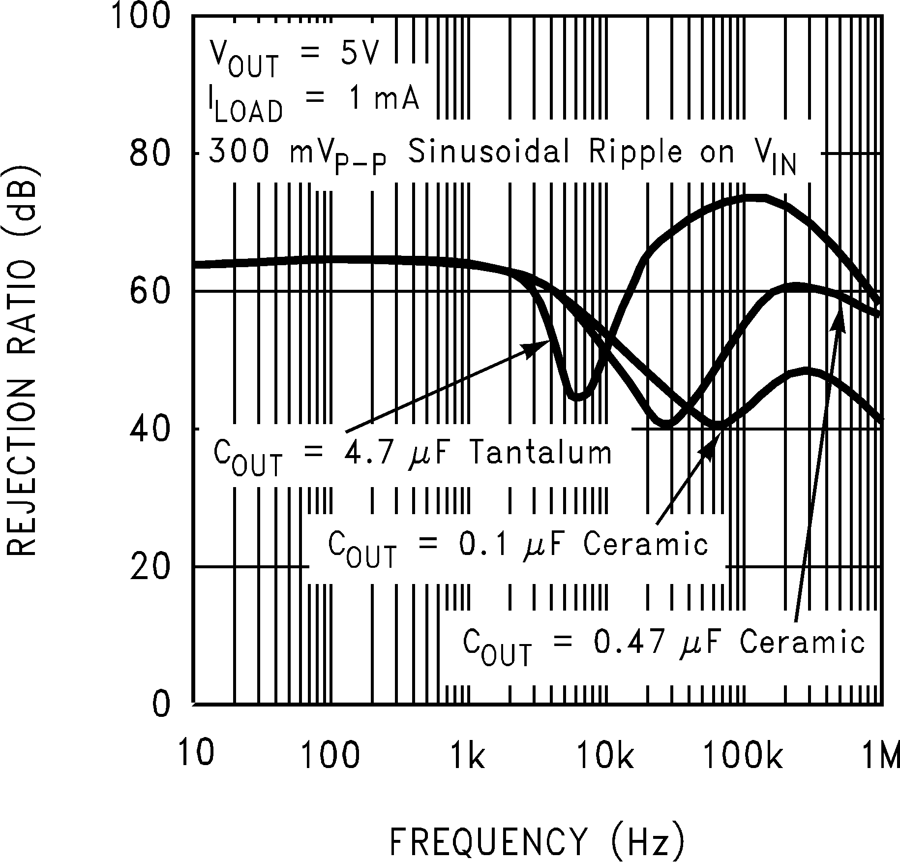 Figure 15. Power Supply Rejection Ratio
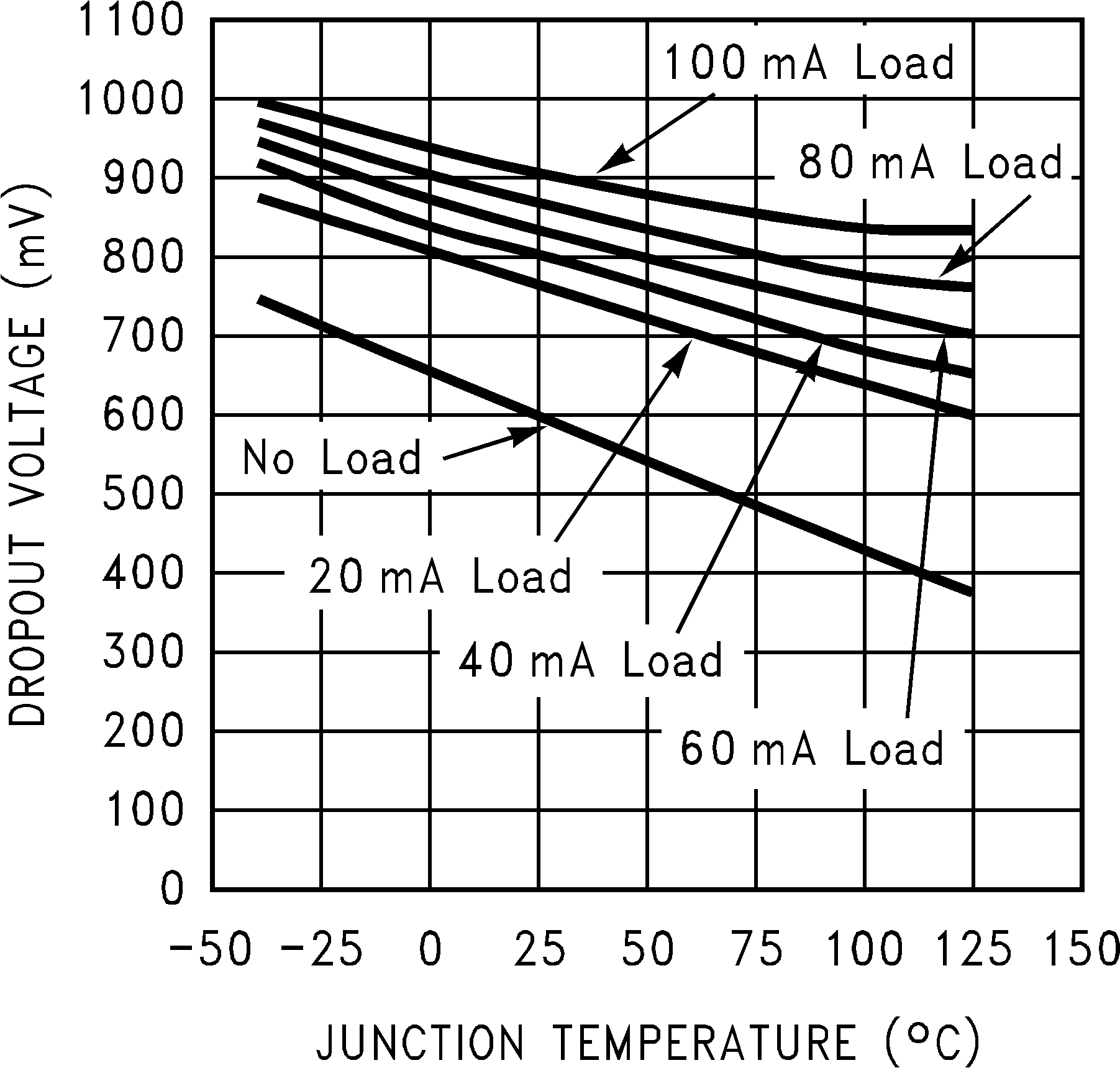 Figure 2. Dropout Voltage vs Junction Temperature
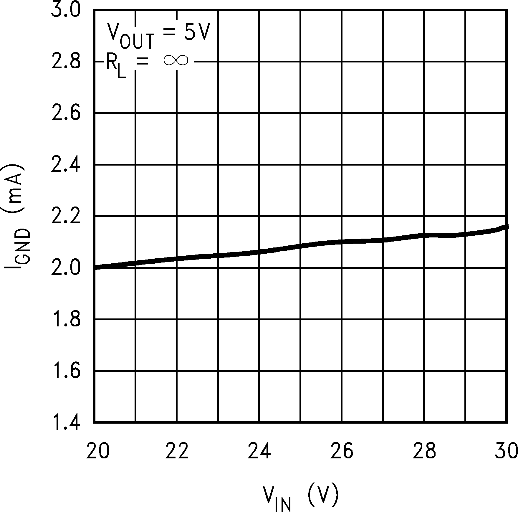 Figure 4. Ground Pin Current vs Input Voltage
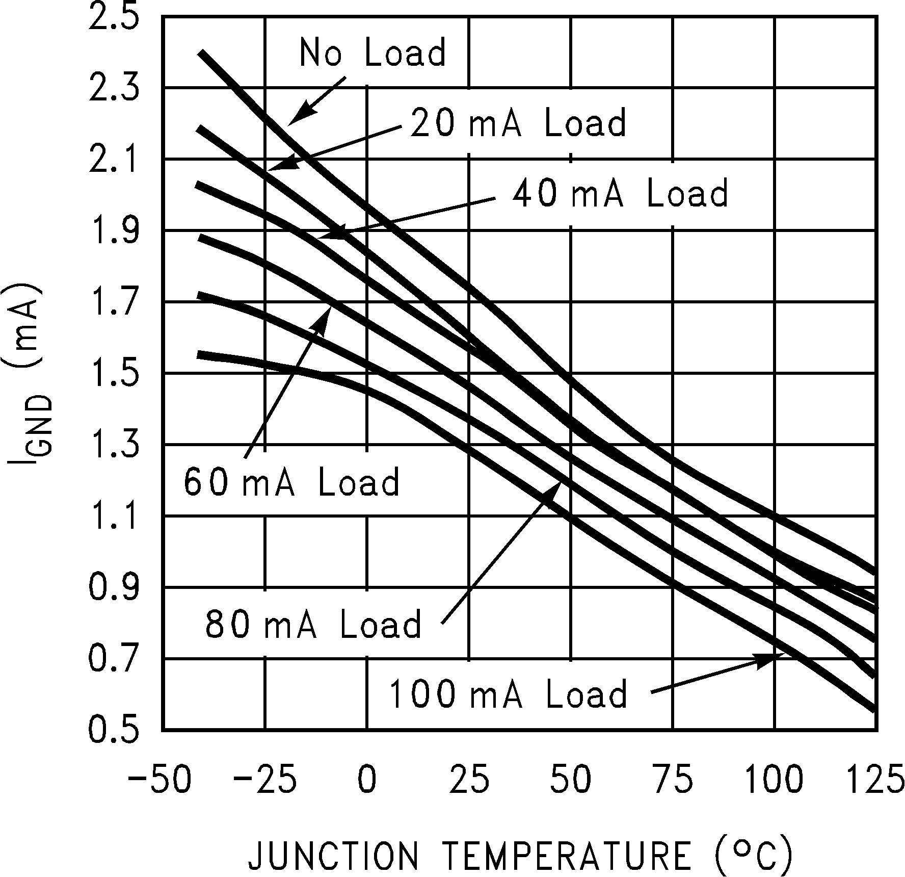 Figure 6. Ground Pin Current vs Junction Temperature
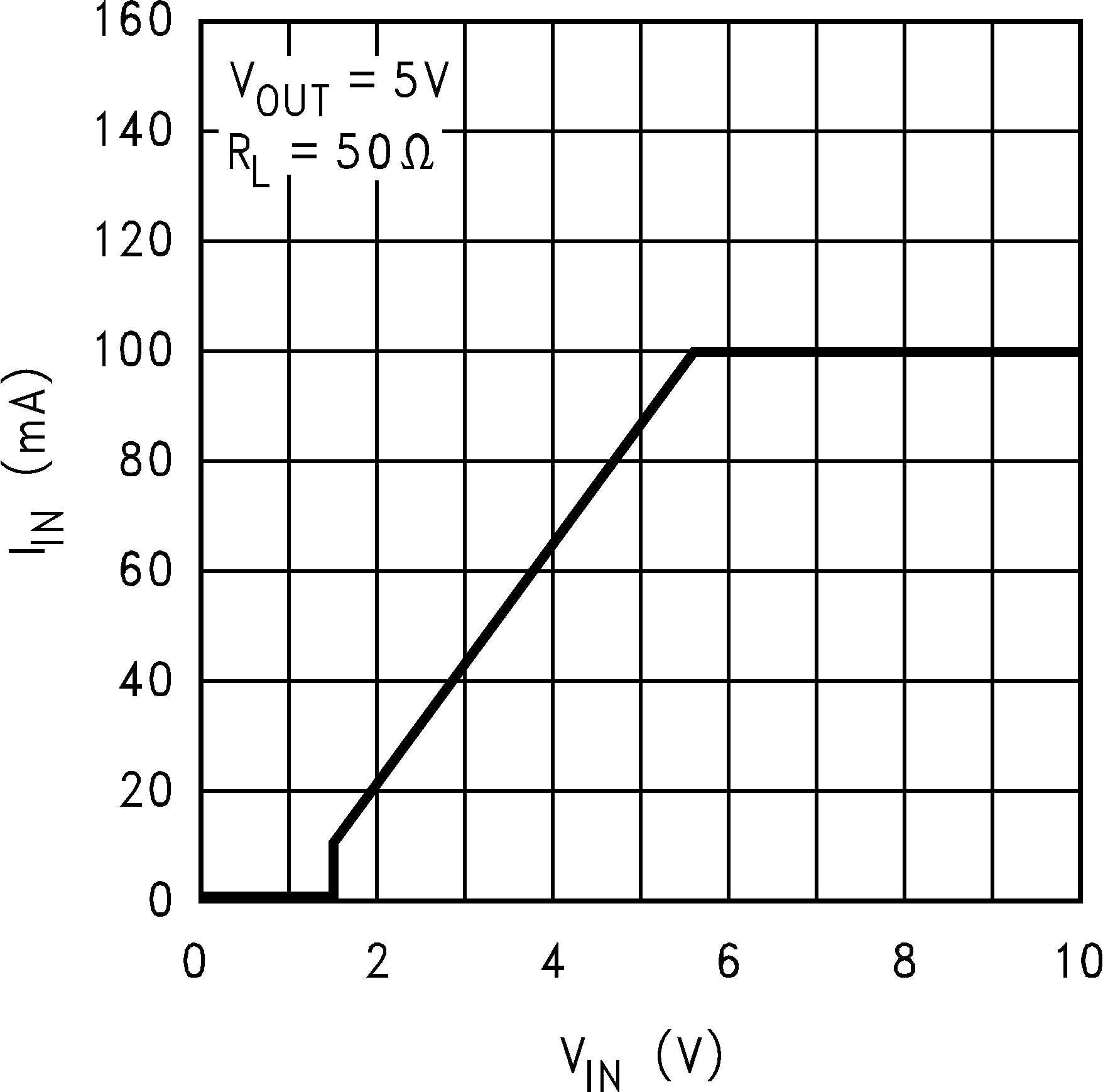 Figure 8. Input Current vs Input Voltage
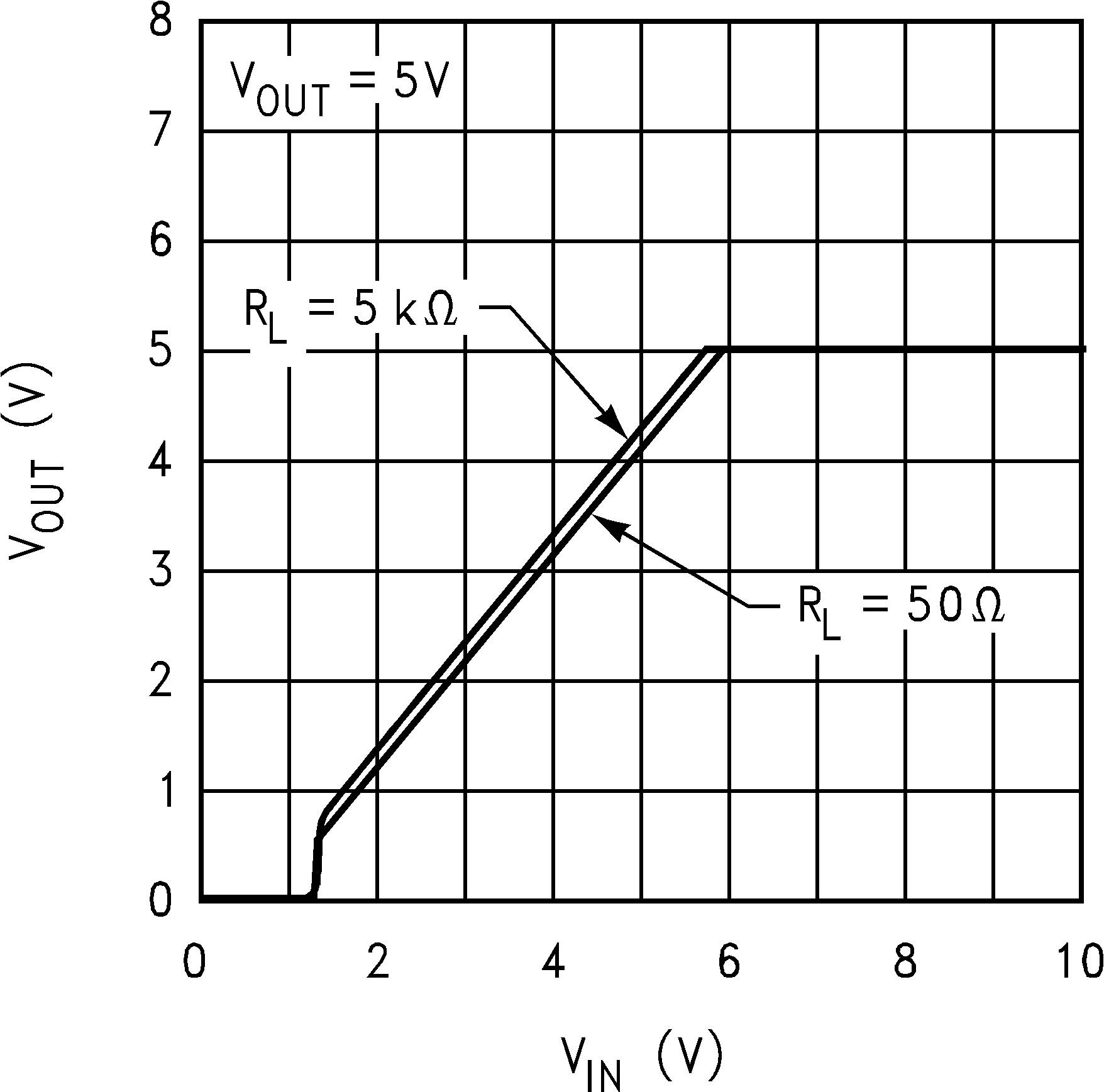 Figure 10. Output Voltage vs Input Voltage
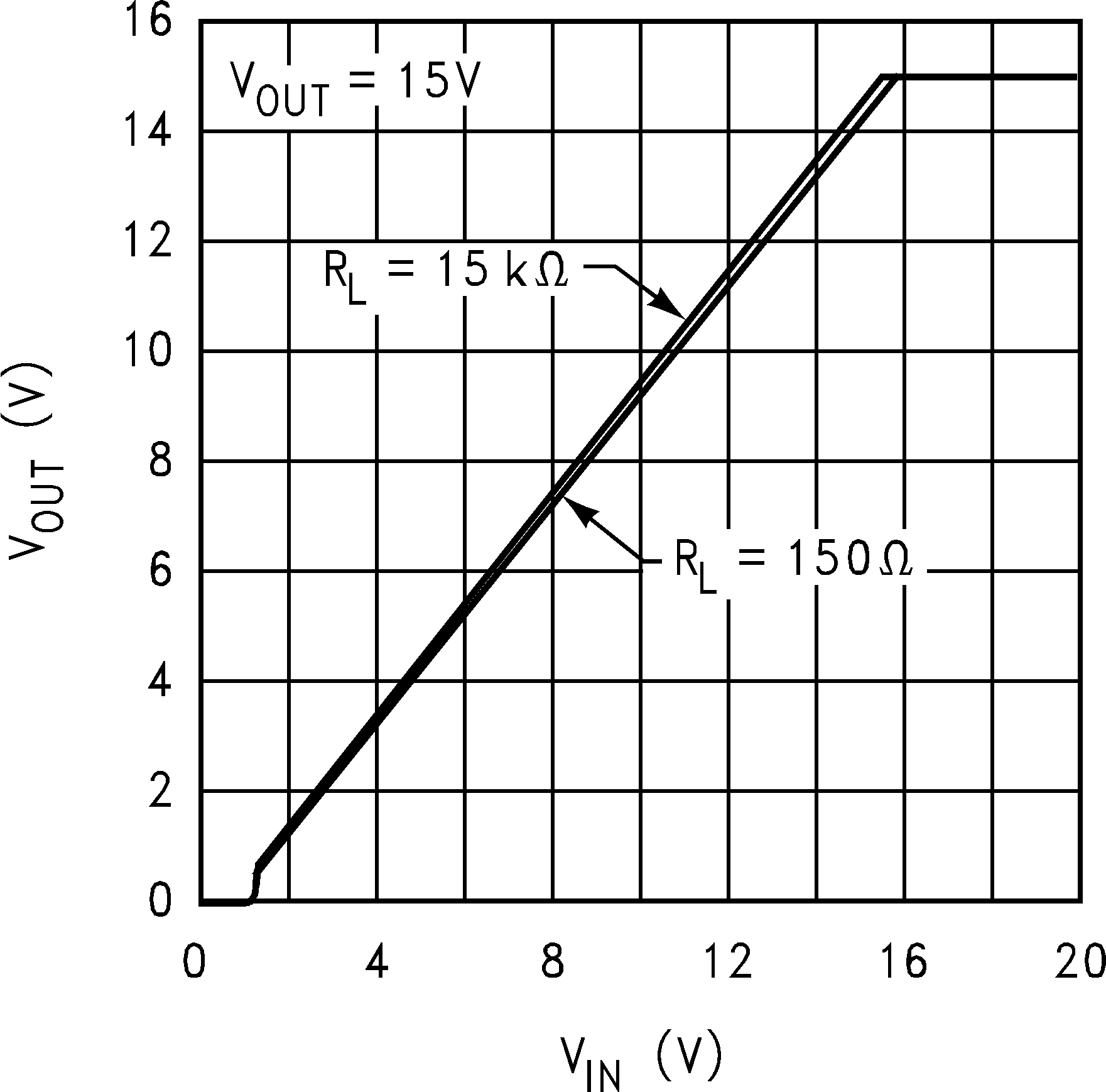 Figure 12. Output Voltage vs Input Voltage
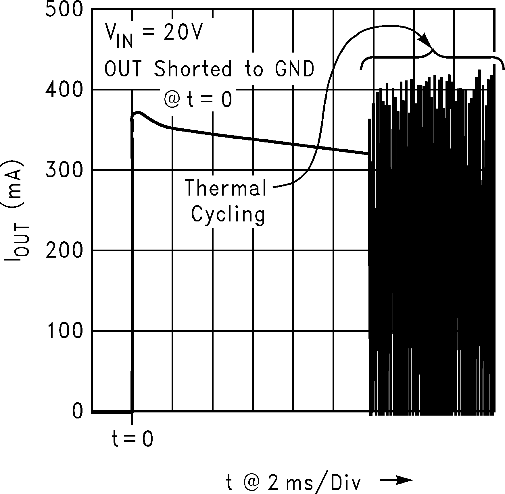 Figure 14. Output Short-Circuit Current
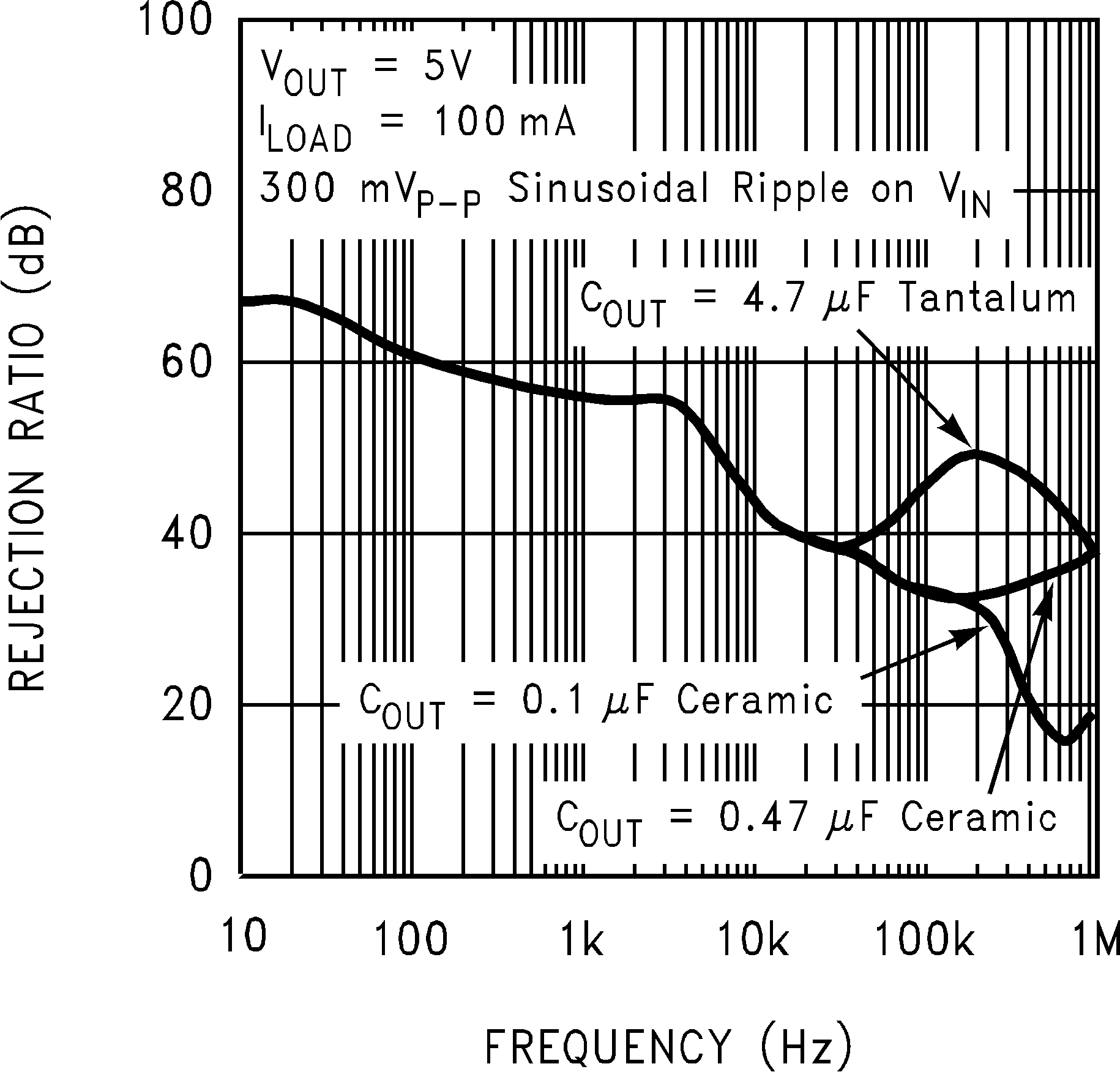 Figure 16. Power Supply Rejection Ratio
