| CURRENT CONSUMPTION |
| ISD |
Shutdown current |
nRST = LOW, LCD_EN = LOW |
|
1 |
|
µA |
| IQ |
Quiescent current, device not switching |
nRST = HIGH, LCD_EN = LOW, 2.7 V ≤ VIN ≤ 5 V |
|
60 |
|
µA |
| ILCD_EN |
|
nRST = HIGH, LCD_EN = HIGH, 2.7 V ≤ VIN ≤ 5 V, no load, Backlight disabled |
|
1 |
|
mA |
| DEVICE PROTECTION |
| UVLO |
Undervoltage lockout |
VIN decreasing |
|
2.5 |
|
V |
| VIN increasing |
|
2.6 |
|
V |
| TSD |
Thermal shutdown(2) |
|
|
140 |
|
°C |
| TSD(hyst) |
Hysteresis(2) |
|
|
20 |
|
°C |
| LED CURRENT SINKS |
| ILED1/2 |
Minimum output current |
Brightness code 0x001 |
|
50 |
|
µA |
| Maximum output current |
Brightness code 0x7FF, exponential mapping |
|
25 |
|
mA |
| Maximum output current |
Brightness code 0x7FF, linear mapping |
|
25.3 |
|
mA |
| IACCURACY |
Absolute LED current accuracy (1) |
2.7 V ≤ VIN ≤ 5.0 V, LED Currents 0.05 mA, 1 mA, 5 mA, 25 mA |
–3% |
|
3% |
|
| IMATCH |
LED1 to LED2 current matching (1) |
2.7 V ≤ VIN ≤ 5.0 V, LED Currents 0.05 mA, 1 mA, 5 mA, 25 mA |
0% |
|
3% |
|
| VHR_MIN |
Current sink saturation voltage |
ILED = 95% of 5 mA |
|
30 |
50 |
mV |
| BACKLIGHT BOOST CONVERTER |
| VOVP_BL |
Backlight boost output overvoltage protection |
2.7 V ≤ VIN ≤ 5 V, 29-V Option |
|
28.8 |
|
V |
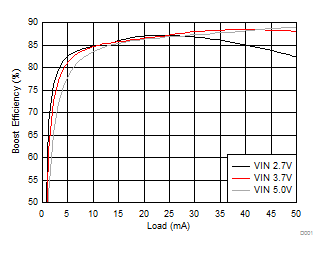
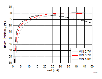
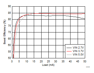
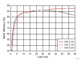
| ηLED_DRIVE |
LED drive efficiency (2) |
ILED = 10 mA/string, 2P6S LED configuration
1235AS-H-220M Inductor |
|
88% |
|
|
| VHR |
Regulated current sink headroom voltage |
ILED = 25 mA |
|
250 |
|
mV |
| ILED = 5 mA |
|
100 |
|
mV |
| RDSON |
NMOS switch on resistance |
ISW = 250 mA |
|
0.5 |
|
Ω |
| ICL |
Selectable NMOS switch current limit |
900-mA setting |
|
900 |
|
mA |
| ƒSW |
Switching frequency |
500-kHz mode |
450 |
500 |
550 |
kHz |
| 1-MHz mode |
900 |
1000 |
1100 |
| DMAX |
Maximum duty cycle |
|
|
94% |
|
|
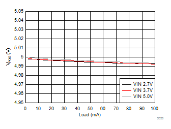
| LCD BIAS BOOST CONVERTER |
| VOVP_BST |
LCD bias boost output overvoltage protection |
|
|
6.8 |
|
V |
| ƒSW_BST |
Switching frequency (2) |
Load current 100mA |
|
2500 |
|
kHz |
| VBST |
Minimum Bias boost output voltage |
LCD_BST_OUT = 000000b |
|
4.5 |
|
V |
| Maximum Bias boost output voltage |
LCD_BST_OUT = 100101b |
|
6.35 |
|
| Output voltage step size |
|
|
50 |
|
mV |
| Peak-to-peak ripple voltage (3) |
ILOAD = 50 mA, CBST = 10 µF |
|
50 |
|
mVpp |
| BST_OUT line transient response (3) |
VIN + 500 mVp-p AC square wave, Tr = 100 mV/µs, 200 Hz, 12.5% Duty, ILOAD 5 mA, CIN = 10 µF, CBST = 10 µF |
–50 |
±25 |
50 |
mV |
| BST_OUT load transient response (3) |
Load current step 0 mA - 150 mA, TRISE/FALL = 100 mA/µs, CIN = 10 µF, CBST = 10 µF |
–150 |
|
150 |
mV |
| ICL_BST |
Valley current limit |
|
|
1000 |
|
mA |
| RDSON_BST |
High-side MOSFET on resistance |
TA = 25°C |
|
170 |
|
mΩ |
| Low-side MOSFET on resistance |
TA = 25°C |
|
290 |
|
| ηBST |
Efficiency (2) |
80 mA < IBST < 200 mA |
|
92% |
|
|
| tST_BST |
Start-up time (BST_OUT), VBST_OUT = 10% to 90% (3) |
CBST = 20 µF |
|
|
1000 |
µs |
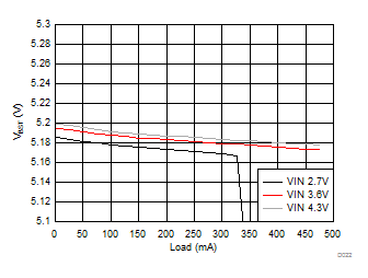
| LCD POSITIVE BIAS OUTPUT (LDO_VPOS) |
| VPOS |
Minimum output voltage |
LDO_VPOS_TARGET = 000000b |
|
4.0 |
|
V |
| Maximum output voltage |
LDO_VPOS_TARGET = 101000b |
|
6.0 |
|
V |
| Output voltage step size |
|
|
50 |
|
mV |
| Output voltage accuracy |
Output voltage = 5.4 V, ILOAD= 1 mA |
–1.5% |
|
1.5% |
|
| LDO_VPOS line transient response (3) |
VIN + 500 mVp-p AC square wave, Tr = 100 mV/µs, 200 Hz, ILOAD 25 mA, CIN = 10 µF |
–25 |
|
25 |
mV |
| LDO_VPOS load transient response (3) |
5 mA to 100 mA load transient, TRISE/FALL = 2 µs , CVPOS = 10 µF |
–100 |
|
100 |
mV |
| DC load regulation (3) |
1 mA ≤ ILOAD ≤ 100 mA |
|
|
20 |
mV |
| PGRISING |
Power-good threshold, voltage increasing |
% of target VPOS |
|
95% |
|
|
| PGFALLING |
Power-good threshold, voltage decreasing |
% of target VPOS |
|
90% |
|
|
| IPOS_MAX |
Maximum output current |
|
|
100 |
|
mA |
| ICL_VPOS |
Output current limit |
|
|
200 |
|
mA |
| IRUSH_PK_VPOS |
Peak start-up inrush current (3) |
VBST = 6.3 V, VPOS = 6 V, CVPOS = 10 µF |
|
500 |
|
mA |
| VDO_VPOS |
LDO_VPOS dropout voltage (4) |
ILOAD = 100 mA, VPOS = 4 V |
|
80 |
|
mV |
| PSRRVPOS |
Power supply rejection ratio, LDO_VPOS (3) |
ƒ = 10 Hz to 500 kHz, ILOAD= 50 mA, VBST to VPOS, 300 mV minimum headroom |
|
25 |
|
dB |
| tST_VPOS |
Start-up time LDO_VPOS, VLDO_VPOS = 10% to 90% (3) |
CVPOS = 10 µF |
|
|
1 |
ms |
| RPD_VPOS |
Output pull-down resistor, LDO_VPOS |
LDO_VPOS pull-down enabled, LDO_VPOS disabled |
52 |
80 |
110 |
Ω |
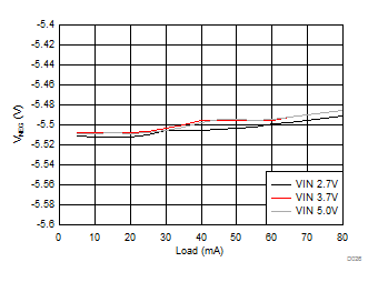
| LCD NEGATIVE BIAS OUTPUT (CP_VNEG) |
| VOVP_VNEG |
LCD bias negative charge-pump output overvoltage protection |
Below VNEG output voltage target |
|
–250 |
|
mV |
| VSHORT_VNEG |
LCD bias negative charge-pump output short circuit protection |
|
|
–1 |
|
V |
| VNEG |
Minimum output voltage |
CP_VNEG_TARGET = 101000b |
|
–6.0 |
|
V |
| Maximum output voltage |
CP_VNEG_TARGET = 000000b |
|
–4.0 |
|
V |
| Output voltage step size |
|
|
50 |
|
mV |
| Output accuracy |
Output voltage = –5.4V |
–1.5% |
|
1.5% |
|
| Peak-to-peak ripple voltage (3) |
ILOAD = 50 mA,
CVNEG = 10 µF |
|
60 |
|
mVpp |
| CP_VNEG line transient response (3) |
VIN + 500 mVp-p AC square wave, 100 mV/µs 200 Hz, 12.5% DS at 5 mA |
–50 |
±25 |
50 |
mV |
| CP_VNEG load transient response (3) |
5 mA to 50 mA load transient, TRISE/FALL = 1 µs, CVNEG = 10 µF |
–100 |
|
100 |
mV |
| PGRISING |
Power good increasing |
% of Target VNEG |
|
95% |
|
|
| PGFALLING |
Power good decreasing |
% of Target VNEG |
|
90% |
|
|
| ηCP |
Efficiency(2) |
VIN = 3,7V, VBST = 5,7V VNEG = -5.4V, 20mA < ILOAD < 80mA |
|
92% |
|
|
| INEG_MAX |
Maximum output current (3) |
VIN = 3.7 V, VBST = 5.6 V,
VNEG = –5.4V |
|
50 |
|
mA |
VIN = 3.7 V, VBST = 5.7 V,
VNEG = –5.4 V |
|
80 |
|
mA |
| ICL_VNEG |
Output current limit (3) |
|
|
150 |
|
mA |
| tST_VNEG |
Start-up time, CP_VNEG, VCP_VNEG = 10 % to 90 % (3) |
VNEG = –6V, CVNEG = 10 µF |
|
|
1 |
ms |
| RPU_VNEG |
Output pull-up resistor, CP_VNEG (3) |
CP_VNEG Pull-Up Enabled, CP_VNEG Disabled, VBST > 4.8V |
|
30 |
40 |
Ω |
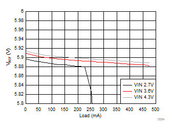
| LCD GAMMA REFERENCE OUTPUT (LDO_OREF) |
| VOREF |
Minimum Output voltage |
LDO_OREF_TARGET = 000000b |
|
4.0 |
|
V |
| Maximum Output voltage |
LDO_OREF_TARGET = 101000b |
|
6.0 |
|
V |
| Output voltage step size |
|
|
50 |
|
mV |
| Output accuracy |
ILOAD_LDO_OREF < 5 mA, VOREF= 5.4V |
–1.5% |
|
1.5% |
|
| LDO_OREF line transient response (3) |
VIN + 500 mVp-p AC Square Wave, 100 mV/µs 200 Hz at 5 mA, CIN = 10 µF |
–50 |
|
50 |
mV |
| LDO_OREF load transient (3) |
5 mA to 50 mA load transient @ 2 µs TRISE/FALL, CIN = 10 µF |
–50 |
|
50 |
mV |
| DC load regulation (3) |
1 mA ≤ ILOAD_LDO_OREF ≤ ILOAD_LDO_OREF_MAX |
|
|
20 |
mV |
| PGRISING |
Power good increasing |
% of target VLDO_OREF |
|
95% |
|
|
| PGFALLING |
Power good decreasing |
% of target VLDO_OREF |
|
90% |
|
|
| IOREF_MAX |
Maximum output current |
|
|
50 |
|
mA |
| ICL_OREF |
Output current limit |
|
|
80 |
|
mA |
| IRUSH_PK_OREF |
Peak start-up inrush current (3) |
VBIASBST = 5.8 V, VOREF = 5.5 V, COREF = 10 µF |
|
250 |
|
mA |
| VDO_OREF |
LDO_OREF dropout voltage (5) |
ILOAD_LDO_OREF = ILOAD_LDO_OREF_MAX, VLDO_OREF = 4.0 V |
|
80 |
|
mV |
| PSRROREF |
Power supply rejection ratio, LDO_OREF (3) |
F = 10 Hz to 500 kHz @ Imax/2, VBST_OUT to VLDO_OREF, 300 mV minimum headroom |
|
25 |
|
dB |
| tST_OREF |
Start-up time, LDO_OREF, VLDO_OREF = 10% to 90% (3) |
COREF = 10 µF, VLDO_OREF = 5.5 V |
|
|
1 |
ms |
| RPD_OREF |
Output pull-down resistor, LDO_OREF |
LDO_OREF pull-down enabled, LDO_OREF disabled |
130 |
200 |
270 |
Ω |
| LCD CONTROLLER SUPPLY OUTPUT (LDO_CONT) |
| VCONT |
Output voltage |
LDO_CONT_VOUT = 00 |
|
1.8 |
|
V |
| LDO_CONT_VOUT = 01 |
|
2.3 |
|
| LDO_CONT_VOUT = 10 |
|
2.8 |
|
| LDO_CONT_VOUT = 11 |
|
3.3 |
|
| Output accuracy |
Output Voltage = 1.8 V, 1-mA load |
–2% |
|
2% |
|
| LDO_CONT line transient response (3) |
VIN + 500 mVp-p AC Square Wave, 100 mV/µs 200 Hz at 5 mA |
–50 |
|
50 |
mV |
| LDO_CONT load transient response (3) |
5-mA to 80-mA load transient @ 2 µs TRISE/FALL |
–50 |
|
50 |
mV |
| DC load regulation (3) |
1 mA ≤ ILOAD_LDO_CONT ≤ 80 mA |
|
|
20 |
mV |
| ICONT_MAX |
Maximum output current |
|
|
80 |
|
mA |
| ICL_CONT |
Output current limit |
|
|
130 |
|
mA |
| VDO_CONT |
LDO_CONT dropout voltage (6) |
ILOAD = 80 mA, VCONT = 3.3 V |
|
|
80 |
mV |
| PSRRLDO_CONT |
Power supply rejection ratio, LDO_CONT (3) |
F = 10 Hz to 500 kHz @ Imax/2 VIN to VLDO_CONT, 300-mV minimum headroom |
|
25 |
|
dB |
| tST_CONT |
Start-up time, LDO_CONT, VCONT = 10% to 90% (3) |
VCONT = 1.8 V |
|
|
1 |
ms |
| RPD_CONT |
Output pull-down resistor, LDO_CONT |
LDO_CONT pull-down enabled, LDO_CONT disabled |
|
200 |
|
Ω |
| LOGIC INPUTS (PWM, NRST, LCD_EN, SCL, SDA, OTP_SEL) |
| VIL |
Input logic low |
|
0 |
|
0.4 |
V |
| VIH |
Input logic high |
|
1.2 |
|
VIN |
V |
| IINPUT |
Logic input current |
|
–1 |
|
1 |
µA |
| LOGIC OUTPUTS (SDA, FLAG) |
| VOL |
Output logic low |
IOL = 3 mA |
0 |
|
0.4 |
V |
| ILEAKAGE |
Output leakage current |
|
|
|
1 |
µA |
| PWM INPUT |
| ƒPWM_INPUT |
PWM input frequency |
|
100 |
|
20000 |
Hz |
| tMIN |
Minimum PWM ON/OFF time |
|
|
400 |
|
ns |
| tTIMEOUT |
PWM timeout(3) |
|
|
24 |
|
ms |
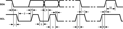 Figure 1. I2C Timing Parameters